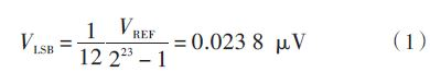
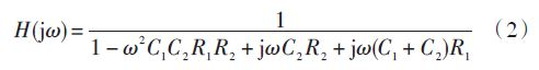
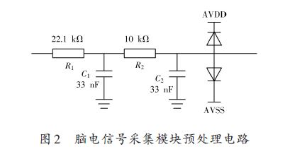
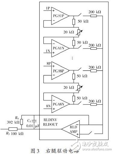
Electroencephalogram (EEG) is a typical bioelectrical signal, which is an overall reflection of the electrical activity of cerebral cortical neurons. It contains a large amount of physiological and pathological information and is one of the important physiological parameters for clinical detection. An important means of research in the fields of science, brain-computer interface and alertness. Since the traditional EEG signal acquisition devices are relatively large and inconvenient to obtain timely EEG signals, it is of great significance to study portable EEG signal acquisition devices. The EEG signal acquisition system mainly includes signal amplification and conditioning, analog-to-digital conversion, signal processing and transmission. Because the impedance of the human body is high and the change is large, the EEG signal is very weak, and the interference of the external environment is very large. Therefore, the amplification and conditioning circuit of the EEG signal acquisition system is complicated, and usually includes a high input impedance and a high common mode rejection ratio. Preamplifier, bandpass filtering, power frequency notch, multi-stage amplification, etc., resulting in high volume and high power consumption. The accuracy and rate of analog-to-digital conversion also determine the performance of the EEG signal acquisition system, using a 10-bit analog-to-digital conversion chip, or using the ADI's 12-bit AD1671 chip with a maximum sampling rate of 1.25 MBPS, or 16-bit A/D conversion. chip. In a system using a single chip microcomputer, an ARM, and a DSP as a control device, generally only a single function of data acquisition and processing can be completed, and the data processing capability of the DSP is the strongest. In contrast, using FPGA as the main control chip can be flexibly configured through hardware description language programming, enabling parallel processing of multi-channel data, and enabling multiple functions to be implemented on a single chip. The integration is based on FGPA and ADS1258. An evoked potential meter with visual, auditory, and somatosensory stimulus sources and a 16-channel EEG signal acquisition function. The means of EEG signal transmission is mainly wired such as PCI bus and USB, and the wireless mode has a low transmission rate, but is more portable and can be targeted for a specific application. ADS1298 is a 24-bit dedicated analog-to-digital conversion chip that TI has introduced in recent years for ECG and EEG signal acquisition. This paper uses the high precision of this chip to use FPGA as the main control chip, by trapping the power frequency and bandpass. The analog part such as filtering is transferred to the digital side, and the analog circuit for enlarging and conditioning the EEG signal is simplified under the premise of ensuring performance, and the acquisition of the portable EEG signal is realized. 1 system structure The EEG signal acquisition system proposed in this paper includes three parts: signal acquisition, analog-to-digital conversion and data transmission. The overall block diagram of the EEG signal acquisition system is shown in Figure 1. The pre-processing circuit includes RC low-pass filtering and overvoltage protection circuit. The signal collected by the brain electrode is low-pass filtered and overvoltage-protected and directly sent to the ADS1298 analog-to-digital converter for analog-to-digital conversion. The right leg drive circuit is mainly used to suppress common mode interference, and is composed of an RLD circuit inside the ADS1298 and an external amplification filter circuit. The system uses FPGA as the main control chip, and uses the hardware descriptive language to write the configuration I/O port into a universal serial SPI interface, and communicates with the SPI interface of the high-precision multi-channel analog-to-digital conversion chip ADS1298 to control the ADS1298. The analog signal collected by the electrode is converted into a digital signal, which is processed by the filter notch and stored in the SDRAM as a buffer part of the collected data to prepare for the subsequent transmission module. The data transmission module mainly uses the FPGA configuration I/O port as the control interface of the Ethernet interface chip DM9000A, and is connected in series with the control interface of the DM9000A to realize its logic control; the data read from the SDRAM is packaged by the UDP protocol through the RJ45. The network interface is transmitted to the host computer. The sampling rate of 8 channels of 1 kHz theoretically requires a transmission rate of 192 Kb/s, and the transmission rate of the Ethernet port 10/100M can fully meet the needs. 2 hardware circuit design 2.1 EEG signal acquisition preprocessing circuit The amplitude of the spontaneous EEG signal of the human body is very small, generally 5~100 μV, and the amplitude of the induced EEG signal is smaller, only about 2 μV. TI's ADS1298 is a 24-bit, 8-channel differential input analog-to-digital converter with a maximum common-mode rejection ratio of 115 dB and a DC input impedance of 1 GΩ with an internal gain of 12 and a reference voltage of VREF = 2.4 V. , the signal resolution is: Therefore, the EEG signal can be satisfied by the simple low-pass filtering and analog-to-digital conversion without amplification and conditioning. Therefore, the pre-processing circuit design is shown in Figure 2. The frequency response function is: It can be seen from equation (2) that the 3 dB cutoff frequency is 96.2 Hz, and the main frequency band of the EEG signal is concentrated from 0.1 to 100 Hz. This preprocessing circuit can completely cover the useful information of the EEG signal. 2.2 right leg drive circuit The right leg drive circuit is the most common and effective method for suppressing common mode interference (especially 50 Hz power frequency) in bioelectric signal acquisition systems. Since the ADS1298 chip integrates the right leg drive circuit, it only needs to configure the ADS1298 internal related registers and use a small number of electronic devices on the periphery to achieve this function. The specific right leg drive circuit is shown in Figure 3. As can be seen from Figure 3, the circuit consists of the RLD circuit inside the ADS1298 and the external R3, R4, C3, of which R3 acts as a current limiting protection, and R4 and C3 form an inverse amplification filter circuit.
lithium-ion battery, LiFePO4 Battery; Lithium Battery, rechargeable battery pack,19inch battery pack, Lithium Battery Pack, Long life Lithium Battery Lithium Battery Lithium Iron Batteries,Lithium Power Supply,LiFePO4 battery Lithium Battery long life battery 12v100AH Lithium Battery Starlight Power Industrial Company Limited , https://www.starlite-power.com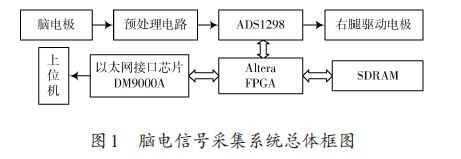
long life battery, battery pack ,12V Solar Battery, battery for 48v system, Lithium Battery bank, LiFePO4 Battery Pack
Lithium Iron Phosphate Battery, li-ion battery pack, marine lithium battery,high discharge lifepo4 battery, storage battery, telecom battery, ev battery, solar battery, UPS Battery
< p> 0 Preface
August 12, 2020