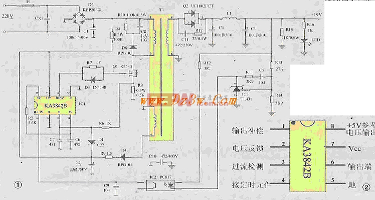
Many electronics enthusiasts who are new to maintenance often find that these notebook adapters with switching power supplies seem more complex and difficult to repair. However, the internal circuit designs of power adapters for various brands and models of notebook computers and LCD monitors are fundamentally similar. For beginners, once they grasp the principle of such a switching power supply, repairing them becomes less daunting. Below, this article takes as an example a typical adapter using the KA3842 control chip in a notebook and LCD power adapter to explain its working principle and maintenance methods. Figure 1 shows the circuit schematic of the adapter's switching power supply. Figure 2 shows the pin functions of the Samsung power supply control chip KA3842 used in the power supply. First, let's discuss the basic working principle of the circuit. The power adapter converts the 220V AC voltage into a 19V DC voltage output, with an output current of approximately 3A. The fundamental working process of the circuit is as follows: the 220V AC input voltage is rectified by the bridge rectifier circuit D2 (KBP206G) and filtered by C1 to produce a DC voltage of around 300V. This voltage is applied to the field-effect switch transistor through the 1-2 winding of the switching transformer T1. The D pole of Ql (K2543) receives one side of the voltage, while the other side is reduced by R4 to obtain approximately 17V of starting voltage to power ICl (KA3842) pin 7, generating a 5V reference voltage from the pin 8 of the internal reference generator of ICl. At this point, the internal oscillator begins to oscillate. From pin 6, a widening pulse (PWM) is output, driving the switching transistor Q1 to operate in the switching state. The D-pole output current of Q1 generates an induced voltage on the primary winding of T1, which is coupled to the magnetic core. The induced voltage generated on the secondary 5-6 winding is rectified and filtered by Schottky diode Q2 and capacitor C4 to obtain a 19V DC voltage output. To ensure the stability of the output voltage, the output terminal is sampled for error correction of the 19V output voltage by R13 and R14. The sampling voltage is compared and amplified for error correction by the three-terminal adjustable shunt reference IC3 (TL431), and drives the optocoupler IC2 (PC817). The error voltage is amplified and sent to the first pin of ICl (KA3842). The width of the output pulse from pin 6 is adjusted by the internal PWM circuit to change the switching time of Q1, thus adjusting the output voltage. Through this feedback control process, the output voltage is ultimately stabilized at 19V. Additionally, there are several overvoltage and overcurrent protections in the circuit: 1. The induced voltage from the primary 3-4 winding of the switching transformer is rectified and filtered by D4 and C2, sending a voltage of about 17V to pin 7 of ICl to maintain the normal operation of IC1 (the 300V voltage is supplied to pin 7 of R4 step-down supply since the current is small as the starting voltage). If the output voltage rises for any reason, the circuit voltage will also rise. When the voltage exceeds 22V, the Zener diode D1 will reverse breakdown, causing the voltage at the overcurrent protection terminal of pin 3 of IC1 to rise above 1V. At this point, IC will be internally shut down, stopping the pulse output from pin 6 of IC1 to achieve overvoltage protection. 2. When the current of switch Q1 becomes too large for some reason, the voltage across the S1 pole of Q1 will increase. When the voltage rises significantly, the voltage at pin 3 of IC1 will also increase. It will then cut off the output of pin 6 of IC1 to provide overcurrent protection. 3. The spike absorption loop formed by R10, C8, and D6 connected to the D pole of switch Q1 absorbs the spike-induced pulse generated on the 1-2 winding of T1 during the Q1 cutoff period, preventing Q1 from being broken down. In practical applications, understanding the role of each component in the circuit is crucial for troubleshooting and repairs. For instance, the KA3842 control chip plays a pivotal role in regulating the output voltage by controlling the duty cycle of the switching transistor. Similarly, the optocoupler ensures isolation between the high-voltage primary side and the low-voltage secondary side, enhancing safety. The use of Schottky diodes and Zener diodes helps manage voltage spikes and stabilize the output, which is especially important in devices like notebook adapters where precise voltage regulation is essential. Overall, while the circuit may appear intricate at first glance, breaking it down into its individual components reveals a well-thought-out design aimed at ensuring both efficiency and reliability. This knowledge empowers technicians to approach repairs with confidence, knowing they can identify and resolve issues systematically. Zgar International (M) SDN BHD , https://www.zgarvape.com