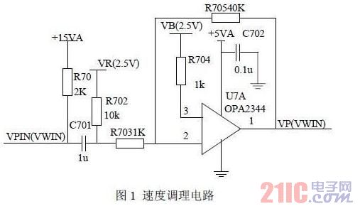
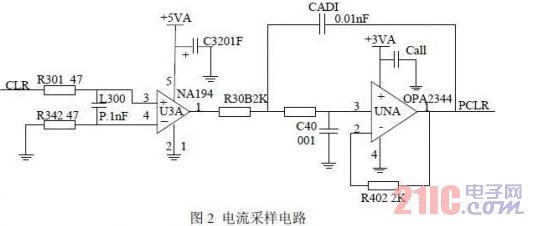
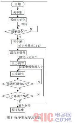
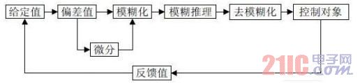
1 Introduction This article refers to the address: http:// The racing brake system is a relatively independent subsystem on the racing system. It is used to withstand the static weight of the car, dynamic impact loads and kinetic energy when absorbing the brakes of the car to achieve braking and control of the car. Its performance directly affects the car's rapid response, safe braking and survivability, which in turn affects the overall performance of the car. This paper designs the hardware and software of the all-electric anti-skid brake controller of the racing car, and finally studies the control law suitable for the racing brake. 2 system hardware circuit design The racing brake controller consists of an anti-skid controller and a motor drive controller. Both controllers are based on DSP chips. The anti-skid controller is mainly controlled by the slip rate, and outputs a given brake pressure. The DSP chip is used as the CPU, plus the racing wheel and the wheel speed signal conditioning circuit. The motor drive controller mainly adjusts the brake pressure and controls the motor current. It also uses the DSP chip as the CPU, plus the peripheral circuit motor current feedback conditioning circuit, overcurrent protection circuit, brake pressure conditioning circuit, and four sets of three-phase full bridge. The inverter circuit and the like constitute a motor drive controller. 2.1 DSP's minimum system The DSP's minimum system mainly involves memory expansion, JTAG interface configuration, reset circuit, ADC module settings, and clock circuit design. 1. Off-chip memory expansion. The off-chip memory is to compensate for the lack of internal DSP RAM, and it is also convenient to download the program to the off-chip high-speed Static RAM during debugging. The external static random access memory uses CY7C1041CV33. The DSP can use either on-chip program memory or off-chip program memory, as determined by the pin XMP knife MC. JTAG interface. When the program needs to be debugged, the program download is completed through the JTAG interface, which is connected to the parallel port of the PC through the emulator. 2. Reset circuit and clock source module. A low-level reset circuit that generates a power-on reset and a manual reset with a RC circuit generates a reset signal. In addition to a hardware watchdog, its output generates a reset signal WDRST. The two inputs of the power chip are both +5V, and the output is +1.9V and +3.3V power supply for the DSP. The output power supply has two reset signals respectively. When the power supply is unstable or too low, a reset signal will be generated. 3. Hardware configuration of the analog-to-digital conversion ADC module. The analog-to-digital conversion ADC output voltage is 2V, requiring the output to be terminated with a low ESR capacitor of 10μF to the analog ground. If the software is set to external reference mode, ADCREFP can be connected to an external input with a 2V reference voltage and a low ESR capacity of 1μF to 10μF. Otherwise, the accuracy of the AD's internal reference source will be affected. 2.2 Racing front wheel and brake wheel speed signal processing circuit The anti-skid controller is mainly controlled by the slip ratio to prevent the car from slipping. The pressure reference value is adjusted by the deviation of the slip ratio to track the given slip rate. The anti-skid controller must have a conditioning circuit for the front wheel and brake wheel speed signals, mainly to obtain the feedback slip rate. The racing speed signal is replaced by a free-rolling front wheel speed signal. The speed sensor is installed on the front wheel and the brake wheel of the car. When the wheel rotates, the speed sensor generates an AC signal in the form of a sine wave. Each time the wheel rotates, the speed sensor emits a 50-cycle sinusoidal AC signal. The amplitude of the sinusoidal AC signal varies with the speed of the wheel. The signal is a sine wave signal with a bias voltage of 2.5V, a peak value of 0.3V, and a maximum signal amplitude of no more than 5V. The sine wave signal is converted into a square wave of the same frequency and sent to the capture unit of the DSP, and the count value interval ncapture of the adjacent rising edge of the square wave is captured, and the rotational speed value V of the wheel can be calculated. Since the CPUCLK is 150MHz, the capture time base is one of the timers, n is the division factor of the CPUCLK, and the radius of the wheel is the calculation formula of the wheel speed: The conditioning circuit is shown in Figure 1: 2.3 logic signal circuit The motor driver uses ALTERA's MAX7000A series devices to logically process the rotor position of the motor, and selects up to 76 programmable I/0 ports and 100-pin EPM7128AE, which can meet system design requirements. The device EPM7128AE realizes the functions of the three-phase full-bridge inverter circuit trigger signal, over-current protection, forward and reverse, and three-phase full-bridge turn-on and turn-off. There is a logic signal for two motors on a CPLD device EPM7128AE. Since the output of the Hall position sensor CS3020 of the brushless DC motor is an open collector structure, the 2KΩ resistor is pulled up, and the Hall signals SA, SB, SC are sent to the input port of the CPLD. The four terminals of TMS, TCK, TDI and TDO of JTAG interface must be connected with pull-up resistors and then connected to +5V power supply. 2.4 Power drive circuit of brushless DC motor The power drive circuit of the brushless DC motor uses a three-phase full-bridge inverter circuit composed of six N-channel MOSFETs centered on IR's dedicated driver chip IR2130. The input is a power-ground PWM wave that is sent to the input port of the IR2130, and the output controls the N-channel power-driven transistor MOSFET, thereby driving the brushless DC motor. The use of this driving method is mainly the clever use of the power drive chip IR2130 to form a suspended high-voltage side power supply for the "bootstrap" technology, which simplifies the design of the entire drive circuit and improves the reliability of the system. Moreover, the IR2130 driver chip has a built-in deadband circuit, as well as overcurrent protection and undervoltage protection, which greatly reduces the complexity of the circuit design and further improves the reliability of the system. 2.5 Current sampling and overcurrent protection circuit The current of the brushless DC motor is detected by the resistance on the bus of the power drive circuit. The resistance above the busbar is connected in parallel by two 0.01Ω power resistors. The sampling circuit samples the current through the two parallel sampling resistors. The sampling resistor converts the current signal into a voltage signal, and the voltage signal is sent to the current monitoring chip for amplification. Then, it is filtered by the second-order active filter circuit composed of OPA2344, and finally the current feedback signal is directly sent to the A/D converter. The hardware overcurrent protection circuit plays an important role in the normal operation of the system, mainly for the protection of the power device MOSFET and the motor. The system also has a software protection function. The overcurrent signal OVCURX is sent to the input pin of the DSP. When OVCUR is high, the DSP will generate a motor control rotation signal ENABLE to turn off the logic signal to stop the motor. The chip IR2130 itself has overcurrent protection. 2.6 Pressure signal amplifier circuit and its conditioning circuit The pressure signal amplifier uses a differential implementation of the subtraction amplifier circuit, with an ultra-low drift voltage operational amplifier as the core, the amplification factor is 40 times, and the amplifier is also equipped with a function of zero adjustment and sensitivity adjustment. The chip 7809 provides a voltage of +9V for the power chip 7660, and the chip 7660 converts the voltage of +9V to -9V, and the two voltages +9V and -9V simultaneously supply power to the OP07. Since the voltage signal from the voltage signal amplifier ranges from +1V to +5V, and the reference voltage of the A/D module of the DSP is +3.3v, the maximum value of the sampled voltage signal cannot exceed +3.3V. Therefore, the voltage signal is passed through the conditioning circuit to reduce the voltage signal to below +3.3V. The conditioning circuit uses a precision operational amplifier OPA2344 to adjust the voltage signal from +1V to +5V to below +3V. It is necessary to set the amplification factor to 0.6 for the DSP to sample. 3 controller software design The software of the racing brake controller is based on the C language, and the assembly language is appropriately used. Such software writing brings convenience to the whole system software. The C language speeds up the development of DSP programs, and the readability and portability are greatly increased. Program debugging is performed in TI's C2000 Code Composer Studio (CCS) integrated development environment. Due to space limitations, only the system program initialization and the main program flow are introduced here. 1, the system program is initialized. Before running the system program, the DSP clock source, timer, watchdog, AD module, I/O port, capture unit, interrupt, etc. must be initialized to make the system internal resources, peripheral devices and hardware circuits. Match. Before the system is running, all interrupts must be turned off to prevent unnecessary interruptions or program runaways while the program is running. Therefore, after initialization, the system will start the interrupt and make the program run normally. 2. The main program flow of the system. The main program of the all-electric brake system of the racing car includes a program initialization module, a timer interrupt service, an analog timing sampling module, a speed signal capture module, a slip ratio control module, a pressure adjustment module, a current adjustment module, and the like. Among them, the timer interrupt service program provides a fixed clock trigger to the current, pressure, and slip ratio modules, and this time is used as the adjustment reference for each module. When the program runs, first shut down the total interrupt of the system, complete the initialization, after receiving the brake command, turn on the total interrupt, enter the infinite loop of program adjustment, until the end of the program run. The current loop adjustment time is the shortest and the fastest. The adjustment time is related to the current signal filtering parameters, DSP sampling speed, CPU clock cycle, software filter program, etc. The general time is a few milliseconds. The time of the pressure regulation ring is set to N times of the current adjustment ring, and the number of adjustments of the current adjustment ring and the pressure adjustment ring can be determined by measuring the adjustment time on site, and the slip rate adjustment time is longer. The main program flow chart of the system is shown in Figure 3. 4 system fuzzy control strategy The fuzzy controller is a key part of the application of fuzzy control in the control system. The main process is to obfuscate the precise quantity of the controlled process output in the obtained system control loop and as the input of the fuzzy controller. The input and output of the fuzzy controller are the actual exact quantities. Then, fuzzy reasoning is performed, and a language-based fuzzy control rule is established internally, and the fuzzy output is judged by the input condition. Finally, the amount of blur is converted into the actual exact amount, that is, defuzzification. The specific process of the fuzzy controller design is shown in Figure 4. Figure 4 Schematic diagram of fuzzy controller The author of this article is innovative This paper mainly completed the design of the racing brake control system, mainly the hardware design, software design and control strategy research. The hardware design uses a high-speed DSP chip and CPLD and designs its peripheral circuits. The system also designed the drive circuit with IR2130 as the core, current signal hardware amplification circuit, filter circuit and protection circuit, pressure signal amplification circuit and filter circuit, racing speed and wheel speed processing circuit and so on. The control strategy uses fuzzy control to adjust the PID parameters.
Led rear view backup camera come with infrared or white LED , really help you checking blind spots in darkness, make you parking and reversing more convenient.
Backup Camera For Car,Led Rearview Backup Camera,Led Car Backup Camera,Led Hd Backup Camera Shenzhen Sunveytech Co.,LTD , https://www.sunveytech.com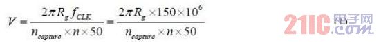

October 08, 2019