On how to borrow SEPIC circuit topology to improve LED system performance
Whether it is in recent years or in the future, light-emitting diode (LED) lighting is a bright star application with high commercial market potential, and driving high-brightness LEDs has become a highly discussed hot topic. For more than one LED application, multiple LEDs can be connected in series to form an LED light string. If the number of LEDs further increases, multiple sets of LED light strings can also be used.
In general, the more common method of driving multiple sets of LED strings is to use a power rectifier and a linear current regulator at the same time. According to the input voltage and output voltage related to the number of LEDs connected in series in the string, a buck or boost circuit is used. Topology. However, if the input voltage is close to the output voltage, the above two circuit topologies are not applicable. This article will introduce the single-ended primary inductance converter (SEPIC) circuit topology to solve this problem, and use this topology technology to design practical application examples for detailed description.
The driver adjusts the LED current according to the dimming frequency
The main function of the LED driver is to control the current flowing through the LED to a stable value, which is expressed by ILED. The value of ILED is related to the color of the LED and depends on the LED. If dimming is required, pulse width adjustment is usually used. Variable (PWM) dimming control, that is, the driver should control the LED current to ILED or 0 according to the dimming frequency. The dimming frequency is generally in the range of 200Hz to 1kHz.
Figure 1 shows an LED driver architecture model diagram with k-string LEDs. The LED driver consists of a power rectifier and k linear current regulators. The input voltage and output voltage of the power rectifier are respectively represented by VIN and VOUT, and each LED string has n LEDs. The voltage drop of each LED string is VLEDi, where the value of i is from 1 to k. VLEDi is the sum of the forward voltage of each LED (VFij), where the value of j is from 1 to n, so the following equation 1:
![]()
Equation 1
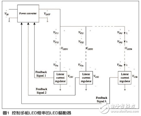
Each LED string is connected between the output of the power rectifier and the linear current regulator (used to control the LED current). The voltage drop of each linear current regulator is represented by VCSi.
Power supply rectifier circuit topology is dominated by voltage
The input voltage and output voltage will dominate the circuit topology of the power rectifier. The output voltage must be higher than the sum of the maximum voltage drop of the LED string (Voltage Drop) and the voltage drop in the linear current regulator, that is, Equation 2
![]()
First, VLEDi is a function of VFij, which represents the forward voltage of the LED. The forward voltage of each LED has a tolerance range and is temperature dependent. For example, when the LED temperature rises, the VFij value generally decreases. When the LED is turned on, the temperature rise value can be calculated. If the ILED value of the LED is 0.35 amps, the typical value and tolerance range of VFij are 3.2 volts and ± 10%, respectively.
Second, VCSi is related to the power of the feedback signal. The VCSi value should be large enough to maintain a good noise ratio of the feedback signal. Linear current regulators also need to have a minimum voltage with proper bias. However, in order to optimize the performance, it is necessary to minimize the value of VCSi, because the power loss value of ith linear current regulator is VCSi & TImes; ILED, which is quite large power. Because ILED is a fixed value, the size of power loss is determined by VCSi, and VCSi is related to VOUT, which can be expressed by Equation 3:
![]()
To illustrate with a practical example, we now have to drive three LED light strings, each with four LEDs, a VLEDi rating of 12.8 volts, and an ILED rating of 0.35 amperes per string. Considering the tolerance range of VLEDi and the minimum voltage drop required by VCSi, the typical design value of VOUT in this example should be 15 volts. If you use a common rechargeable battery with a rated voltage of 12 volts, the battery voltage can change from 10 volts (power is almost exhausted) to 14 volts (power full), and when the battery is fully charged, the voltage value is close to VOUT. Assuming that a boost rectifier is used to obtain a 15V VOUT, if VIN is close to the upper limit (when VIN is 14V, the duty cycle ratio is 6.7%), we only need a lower duty cycle ratio. But in fact, the low duty cycle ratio may not be achieved, because most controllers master the duty cycle ratio or the lower limit of the working time. In this case, the VOUT value must be increased. The result is that the power loss of the linear current regulator increases, which makes The overall efficiency is reduced. Another feasible solution is to reduce the switching frequency to remove the lower limit of working time. However, a low switching frequency will increase the inductor current ripple, which represents the need for larger and more expensive inductors.
For the above applications, the best power rectifier circuit topology is SEPIC, because the input voltage of the SEPIC rectifier can be higher or lower than the output voltage. Other advantages of SEPIC rectifiers include the use of low-side switches (making switch drivers easy to implement) and the output voltage is non-inverting.
LED driving equipment SEPIC helps improve performance
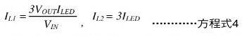
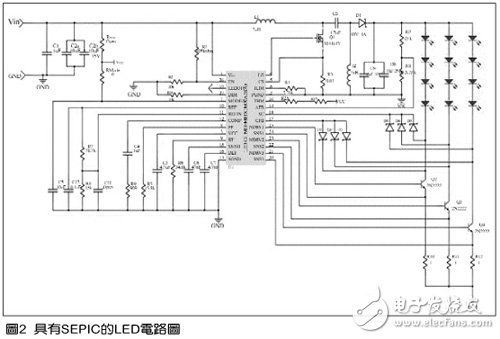
Figure 2 shows the circuit diagram of the LED driver composed of the power rectifier flutter, linear current regulator and controller IC (LM3431) using the SEPIC circuit. The main components of the SEPIC rectifier include two inductors L1, L2, two capacitors CS, C8, MOSFET Q1, and diode D1. When Q1 is turned on, L1 and L2 are charged by VIN and VCS (voltage through CS), and at the same time, CS and C8 are discharged by IL2 (inductor current of L2) and output current (overall LED current). When Q1 is off, L1 and L2 discharge, and CS and C8 charge. Some basic equations in steady state are listed below. The input current is equal to IL1, which is the current value of inductor L1. Since there are three LED light strings, the output current is 3ILED, and IL1 and IL2 can be calculated by the following equation 4:
D represents the working period, TSW is the switching period, ton is the working time of Q1, IL1, ripple and IL2, ripple is the inductor current ripple of L1 and L2, Equation 5 is as follows:
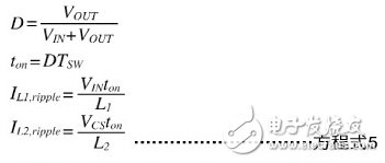
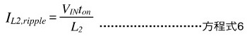
In the steady state, VIN = VCS, so the inductor current ripple of L2 can be expressed by the following equation 6:
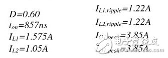
To maintain continuous conduction mode (CCM) operation, even when VIN is at its highest value, L1 and L2 should be large enough to ensure that the inductor current is greater than half of the inductor current ripple. In the example, the switching frequency is 700kHz and the switching period is 1.43μs. When the maximum value of VIN is 14V, VOUT and ILED are 15V and 0.35A, respectively.

To maintain CCM operation, the maximum values ​​of IL1, ripple and IL2 should be 2.25 amps (IL1 & TImes; 2) and 2.1 amps (IL2 & TImes; 2). The minimum values ​​of L1 and L2 are 4.6μH and 4.9μH, respectively. Since the tolerance range of the inductor can be as high as 30%, the choice of L1 and L2 can be 7μH (4.9μH ÷ 0.7).
With IQ1, peak and ID1, peak represent the peak current of Q1 and D1 respectively, equations 7 and 8 are as follows:
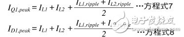
The components of Q1 and D1 should be able to handle the peak current. The maximum value of the peak current often occurs at the lowest value of VIN. In this example, when VIN is 10 volts, both L1 and L1 are 7 μH.
Linear current regulators include current-sense resistors, power transistors, and amplifiers (embedded in the controller IC). The output of the amplifier controls the power transistor (2N2222), and then the current of the LED string is controlled to 0.35 amps, and the current is sensed by a 1 ohm (Ω) resistance. The sense signal is fed back to the input of the amplifier for comparison with the reference voltage of 0.35 volts. 0.35 volts is a voltage divider circuit formed by R7 and R8, which divides the internal reference voltage from 2.5 volts.
A USB Flash Drive, also variously known as a thumb drive, pen drive, gig stick, flash stick,jump drive, disk key, disk on key, flash-drive, memory stick, USB stick or USB memory, is a data storage device that includes flash memory with an integrated USB interface. It is typically removable, rewritable and much smaller than an optical disc. USB Flash drives are often used for the same purposes for which floppy disks or CDs were once used; i.e. for storage, data back-up and transfer of computer files. They are smaller, faster, have thousands of times more capacity, and are more durable and reliable because they have no moving parts.
USB Flash Drive
USB Flash Drive,USB Flash,Pendrive USB,USB Key
Custom Usb Gift company limited , https://www.customusbgift.com