When the ARCNET protocol is applied to the high-speed EMU train communication network, the timing mismatch problem between the central control unit processor PXA270 and the dedicated protocol control device COM20020 is generated. If the general digital circuit module is used for timing conversion, the PXA270 needs to occupy the PXA270 special resources ( CPU time slice) Low-speed read and write access to COM20020 registers and packet buffers (at least 300 ns between adjacent reads of COM20020), which increases the burden on the processor. Based on this situation, an FPGA-based PXA270 peripheral timing conversion interface design scheme is proposed. The FPGA is used as a bridge for timing conversion, and the memory direct access DMA (Direct Memory Aeeess) function is added, that is, the FPGA automatically completes the data packet transmission and reception work. The PXA270 requires only high-speed read and write access to the synchronous dual-port RAM in the FPGA. The FPGA is used to connect the PXA270 processor and peripherals to solve the timing mismatch when the PXA270 processor is directly connected to the peripheral. As shown in Figure 1, the FPGA obtains the address bus (ADDRBUS[17..14], ADDRBUS[9..0]), chip select signal (SYSCS5), read enable (SYSOE), write enable (SYSWE) from the PXA270 processor. And provide bidirectional data port DATABUS[7..0] (can be modified to 32-bit or 16-bit according to the actual application), interrupt (interrupt); at the same time, FPGA provides COM20020 with specific bus interface, including COM20020_DS, COM20020_CS, COM20020_DIR , COM20020_DATABUS [7..0], COM20020_ADDRBUS[2..0], etc. Easy Electronic Technology Co.,Ltd , https://www.pcelectronicgroup.com
2 timing conversion interface overall design 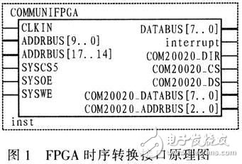
(1) PXA270 writes a register to the peripheral. The PXA270 first sends the data to be written to the dual-port RAM. Then the PXA270 writes a single write command to the specified register of the peripheral to the command register of the FPGA, and then FP-GA. The data in the RAM is output to the peripheral data bus according to the received command, and the write timing to the peripheral is given.
(2) PXA270 single-read operation for peripheral specified register PXA270 first writes a single read instruction to the specified register of the peripheral to the command register of the FPGA. At this time, the FPGA gives the read timing of the peripheral and drives the address of the RAM. A signal such as a bus or a write clock transfers data on the peripheral data bus to the RAM. After a delay of 1 μs, the PXA270 reads data from the RAM.
(3) PXA270 is different from the single-write operation of the peripheral batch data write operation. The PXA270 needs to store the data to be written to the contiguous space of the RAM first, and then write the batch data write operation instruction to the command register of the FPGA. The -GA sends the data in the RAM to the peripheral data bus in a batch according to the received command, and it is necessary to ensure that the write timing to the COM20020 is synchronized with it.
(4) PXA270 peripheral peripheral data read operation is given by the FPGA to the peripheral multiple read timing of the peripheral to send the data in the peripheral to the RAM to complete the storage work. The PXA270 waits for a batch data read completion interrupt to occur after a continuous read of the RAM. 3 functional module design
3.1 Timing Generation Module Design The COM20020 has 80xx-like and 68xx-like bus access methods. Here the 68xx-like access mode is implemented, and Figure 2 shows its read and write access timing.
The common requirement for read and write timing is that the chip select signal CS must be at least 5 ns prior to DS and only allow CS to return to high after DS is inactive; the read/write direction signal DIR should be established at least 10 ns before DS is valid; The DS high level is not less than 20 ns. The different requirements of the two: the address bus of the write timing is established at least 15 ns before the operation pulse DS, and the low level of DS is not less than 20 ns. The valid data of the data bus must be established at least 30 ns before the DS goes high, and keep the DS high. After at least 10 ns; the address bus of the read timing is established at least 15 ns before the chip select signal, the DS low level is not less than 60 ns, and the DS becomes low until the data bus data is valid at intervals of up to 40 ns, and the DS goes high to the data. The high-impedance interval of the bus is up to 20 ns, which is the characteristic that the COM20020 provides as a data output to the access device. For the above requirements of read and write timing, the specific design is as follows: DIR has only one high or low level in one operation, which is given in advance by the command register before the operation, and then gives the enable signal, and DS becomes lower after CS is valid. And goes high before CS is invalid, so that the data is reliably latched. 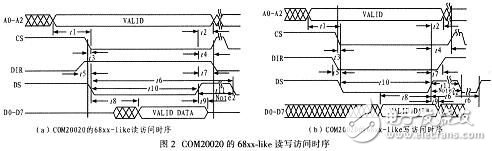
Figure 3 shows the timing diagram of COM20020. From the timing analysis, the following design scheme can be drawn: DIR is used to indicate whether the operation is read or write, DIR='1' is read, otherwise it is write. DIR is assigned before operation; CS is selected when EN is active, and the next rising edge of CLK becomes active. This is for the write operation to prepare data for the COM20020 data bus, does not affect the read operation; DS selects the next CLK rising edge valid for CS to become valid, but gives the rising edge two clock cycles before CS is invalid to meet "The chip select signal CS must be at least 5 ns prior to DS and can only be restored high after DS is inactive" and there should be a clock width of at least 60 ns in the middle of the DS, thus maintaining 3 CLK cycles. Figure 4 is a timing diagram of the CommandGenerator simulation. The counter is used for timing synchronization. The VHDL source code is given below. 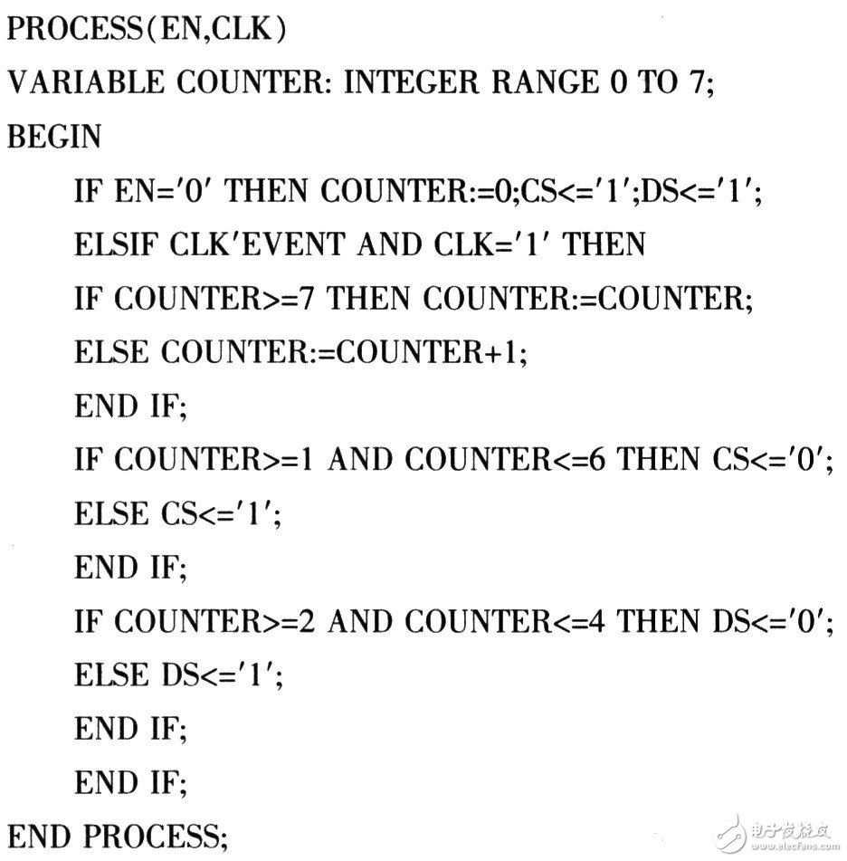
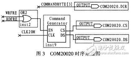
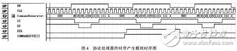
Figure 5 is a schematic diagram of continuous clock generation and automatic address generation for batch data transfer from WRRAM to peripherals. Among them, lpm_counter0 is an increment with asynchronous clear and carry signals; AutoAccessDataNumsOnce generates a batch transfer clock when EN='1', according to the long and short packet transmission requirements of COM20020, transmits long data when CCESSTYPE = '1' Packet (512 B), otherwise a short packet (256 B) is transmitted. The FRE signal simultaneously provides the clock signals of rdRAM and lpm_counter0 of WRRAM. 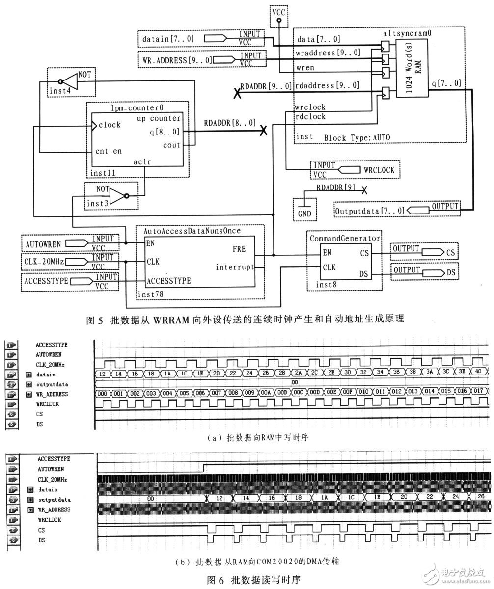
Figure 6 shows the timing simulation of a batch of data written to the RAM, followed by a DMA transfer to send data from the RAM to the COM20020. At the rising edge of WRCLOCK, the RAM stores the data on the datain bus to the byte address space pointed to by WR_AD-DRESS. The WRCLOCK signal is generated by the WE signal of the PXA270 and the chip select signal (active high) assigned to the RAM. And it is. When performing analog write to RAM, it must be ensured that AUTOWREN is invalid (low level); in the RAM output link of verifying data DMA transfer, WRCLOCK should no longer have a rising edge signal to prevent the RAM from being read and written at the same time. In addition, when each data is output from the outputdata port, CS and DS leave enough time for timing generation after a certain delay (1 CLK clock cycle). Need to explain: COM20020 has 2 Kbytes of RAM space inside, which is used to store the data packets to be sent or received. Before writing the data packet to RAM, specify the storage location of the data packet, and then automatically display the pointer in COM20020. Moving position 1, it is only necessary to write data to the RAM continuously without having to give an address signal. 3.3 Specifying Register Operation for Peripherals It is easier to specify register operations for peripherals than for batch data transfer. Simply reduce the number of operations to one and provide the corresponding address for A2 to A0 of COM20020. The specified register operation stores the data in the high 512-byte space of the RAM and only occupies the lower 8 bytes. When programming the PXA270, ensure that the PXA270 is sent to the RAM address and the RAM memory address in the command register is COMMANDBYTE[2. .0] corresponds.
4 Conclusion This design solves the timing matching problem of the ARCNET protocol dedicated device used in the train communication network, and realizes the timing conversion of the PXA270 processor and COM20020. In addition, a reference framework is provided for extending other bus access types. The COM20020 timing in the CommandGenerator can be modified to implement different peripheral bus access types. Modifying the ACCESSTYPE in AutoAccessDataNun-sOnce can configure the data type of the batch data operation.
1 Introduction
November 21, 2021