Lumex is a registered trademark of Lumex, Inc.
Card Reader advantage:
External memory expansion for ipad/ iphone/ ipod touch
Card Reader Card Reader,Card Readers,Mobile Card Reader,Smart Card Reader Dongguan City Leya Electronic Technology Co. Ltd , https://www.dgleya.com
Device OverviewUsing no external components, the MAX6960 LED driver drives two single-color, 8 x 8 dot-matrix digits through its multiplexed 8 row and 16-column ports. A single, open-drain, row port can sink currents from all 16 column ports with a maximum constant sourcing current of 40mA each. These 8 row ports are multiplexed in time; only one row port is activated for current sinking at a given time. The average current through each column port is, therefore, 5mA.
The MAX6960 can also drive a single two-color (red, green) 8 x 8 dot-matrix digit. Each dot-matrix element can be turned on or off individually or have four (including off) intensity levels. The lighting intensity of all digits can be PWM controlled in 256 steps. Up to 256 MAX6960 devices can be daisy-chained to form a larger control unit, whose display memory can be addressed by a host controller through a 4-wire serial interface consisting of DIN, DOUT, CLK , and active-low CS. Another 3-wire interface, consisting of ADDCLK, ADDIN, and ADDOUT used among all the daisy-chained chips, makes the interconnection self-configured; no intervention is needed from the host controller.
The other members of this LED driver family are similar to the MAX6960. The MAX6961 is, however, limited to turning the dot-matrix elements on and off. The MAX6962 can only drive single-color digits. Finally, the MAX6963 turns the dot- matrix elements on and off and can only drive a single-color digit.
Application ExampleFigure 1 shows a simple application using two MAX6960s to drive four single-color digits. The LDM-24288NI is an 8 x 8 green, dot-matrix LED from Lumex®. Four digits (D1, D2, D3, and D4) are placed from left to right to form a display of 8 rows and 32 columns. The column current levels are all set to a constant 40mA because RISET0 and RISET1 of U1 and RISET0 and RISET1 of U2 are all grounded.
The 4-wire interface of U1 and U2 is connected in parallel and not daisy-chained through DIN and DOUT. Only one chip will be selected for individual chip commands because the unique device addresses are configured through the 3-wire interface after power-up . Global commands apply to all MAX6960s simultaneously, which is true when more than two MAX6960s are connected together. The 4-wire interfaces are all connected in parallel.
Each MAX6960 also has a 3-wire interface and all MAX6960s are daisy-chained through this 3-wire interface. One MAX6960 is usually selected as the master. The master has a device address of 0 and generates the clock for the rest of MAX6960s. The ADDCLK pins of all MAX6960s are connected together. Only the master's ADDIN pin is connected to V +. The ADDIN pin of the rest of MAX6960s is connected to the ADDOUT pin of the previous device, whose address is one count lower than its own address. The ADDOUT pin of the last device is left open. 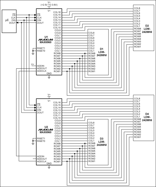
Figure 1. Multiple MAX6960 devices drive four one-color digits.
At power-up, the driver address registers 0x00 of all the MAX6960s are initialized to all zeros, and the ADDOUT pins are set to logic low. The master MAX6960 detects its status because its ADDIN pin is a logic high without the presence of a clock signal. The master then generates the clock signal and raises its ADDOUT to logic high. Each subsequent MAX6960 sets its driver address by counting the clock periods before its ADDIN becomes logic high, and then raises its ADDOUT to logic high. The driver address registers of all the MAX6960s are thus initialized in 256 ADDCLK clock cycles.
Display Memory Address ConfigurationsEach MAX6960 has 64 bytes of display memory that can be divided into two or four intensity planes. Only one plane is selected for driving these ports at a particular time. Multiple planes are available so that a user can have one plane for driving LEDs while updating another. There is also the option of animation by switching through multiple planes.
When using four planes, each plane has 16 bytes or 128 bits for 16 columns by 8 rows of pixels at 1 bit per pixel. In the case of two planes, each plane has 32 bytes or 256 bits, again for 16 columns by 8 rows at 2 bits per pixel. A single-color digit has 8 columns and 8 rows; a two-color digit has 16 columns and 8 rows. A plane can cover two digits for the single-color and one digit for the two-color cases , respectively.
The display memory is accessed 8 bits at a time. For the 1-bit-per-pixel case, when the display memory is written, the first 8 bits are for the first column, the second 8 bits for the second column, etc. A digit of 8 x 8 pixels with one bit per pixel is written in 8 bytes. This means that the address for the first column of the first digit is 0, for the second column of the first digit is 1 ... for the first column of the second digit is 8, etc. When multiple drivers are used, all display memories are combined and the display memory address is determined as follows:
Memory Address = (Driver Number-1) × 16 + (Digit Number-1) × 8 + (Column Number-1)
For the 2-bit-per-pixel case, an 8-bit display memory access only updates half a column. As described earlier, the driver number is automatically configured after power-up through the 3-wire interface and stored in register 0x00. Then 14 bits are used to identify a byte in the combined display memory. The first two bits identify the plane; the remaining 12 bits are used to locate one of 2048 columns among 256 drivers for one bit per pixel. The first bit identifies the plane , and the remaining 13 bits are used to locate one of 4096 half-columns among 256 drivers for 2 bits per pixel.
The MAX6960 only accepts transmissions of 8, 16, or 24 bits through the 4-wire interface. Any transmission that does not contain exactly that number of bits between the falling and subsequent rising edge of active-low CS will be ignored.
Indirect Method to Access RegistersThe display memory address is not needed when the indirect method of 8-bit transmissions is used. There are two, global driver, indirect address registers (0x09 and 0x0A) in each MAX6960. Each of these registers tracks the same global indirect display memory address. At power-up, these registers all start with address 0. After each 8-bit indirect display memory access, registers in all MAX6960s are increased by 1. During an indirect display memory access, each MAX6960 compares the address in these two registers with its own driver address to decide if its display memory needs to be updated.
A user can also access a particular byte in the combined display memory by using the 24-bit transmission. Among these 24 bits, the first bit indicates if it is a write (0) or read (1) operation; the second bit has no meaning and can be ignored; the next 14 bits are used to identify a byte in the combined display memory; and the last 8 bits are the data byte.
The16-bit transmission is used to access 16 registers of the MAX6960s. Among these 16 bits, the first bit indicates if it is a write (0) or read (1) operation; the second determines if the address autoincrement should be activated; the third identifies whether the register access is local (0) or global (1); the fourth should always be 0; the next 4 bits identify which register is intended; and the last 8 bits are the data byte. For a local register access, the driver address is stored at the global driver indirect address register at 0x08. Registers 0x08 of all MAX6960s are initialized to 0 at power-up. They can be changed globally using a 16-bit transmission. They can also be increased simultaneously after each 16 -bit transmission, if the second bit is set.
The MAX6960s might need to be initialized if power-on default values ​​do not meet display size, color, or intensity level specifications. For 256 MAX6960s, register power-on default values ​​are connected in a row with single-color, one-bit- per-pixel, full-digit, and at half-panel intensities.
When using the indirect method, the display memory is accessed one digit (8x8) at a time from the left to the right columns of pixels. The indirect method then moves from the left to right, digit by digit, until the end of a MAX6960 driver row. The method finally sequences MAX6960 driver rows from top to bottom. The indirect method accesses the red memory for the whole display first, and then the green. It is necessary to initialize the global driver devices register at 0x0E, so the display indirect address count can reset itself at the right number. This is illustrated in Figures 2 and 3, where DAN stands for Digit Access Number. A single-digit access updates 8 bytes (an 8 x 8 or 4 x 8 of display matrix for the 1 -bit-per-pixel or 2-bit-per-pixel cases, respectively) of display memory. The global driver devices register should be initialized to the total of number of MAX6960s minus one. 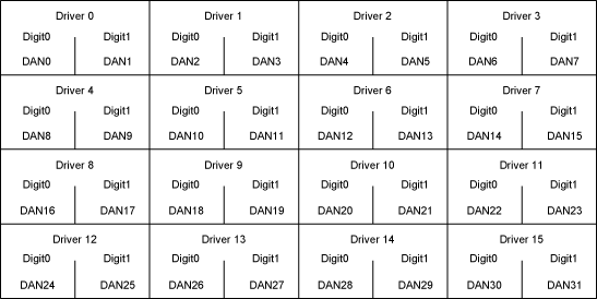
Figure 2. Single-color, 1-bit-per-pixel display memory access sequence. 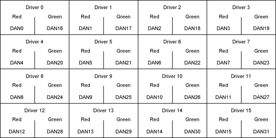
Figure 3. Two-color, 1-bit-per-pixel, display memory access sequence.
It is also necessary to initialize the global driver rows register at 0x0F, if the pixel resolution is 2 bits. This initialization ensures that a MAX6960 row can be accessed first before moving to the next row, as shown in Figures 4 and 5. The global driver rows register should be initialized to the total of number of MAX6960s in a row minus one. 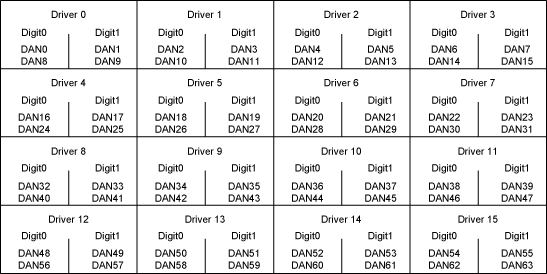
Figure 4. Single-color, 2-bit-per-pixel, display memory access sequence. 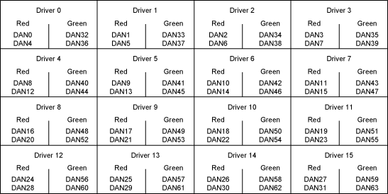
Figure 5. Two-color, 2-bit-per-pixel, display memory access sequence.
Intensity Control Registers The operation details of the MAX6960 are controlled by writing to its 16 registers. These registers include pixel intensity scale (0x01), panel intensity (0x02), digit 0 intensity (0x03), digit 1 intensity (0x04), fault (0x05 ), and global panel configuration (0x0D). There are 8 bits each for these intensity control registers.
Initializing the Global Driver DevicesFollowing are some 16-bit transmissions to initialize the global driver devices and global driver rows registers for the simple application circuit of Figure 1. 0x0E, 0x01, // Write to global driver devices register with two total devices. 0x0F, 0x01, // Write to global driver rows register with two MAX6960s in a row. Following are some 8-bit and one 16-bit transmissions to turn on the edges of the display consisting of four 8 x 8 digits in an 8 x 32 matrix formation with a circuit configuration of Figure 1. 0xFF, // Light up the left edge. 0x81, // Light up top and bottom pixels of the second column. 0x81, // Light up top and bottom pixels of the third column.. .. 0x81, // Light up top and bottom pixels of the fourteenth column. 0x81, // Light up top and bottom pixels of the fifteenth column. 0xFF, // Light up the left edge. 0x0D, 0x31, // Turn on the shutdown bit.
Manage all data directly on the iOS-Device
(create, copy, move, delete, rename, open in and many more)
Playback Videos/Music directly from external memory
Backup and restore your contact list
Document viewer for all major file formats
Voice recorder/ Text editor
Dropbox support
Support ios 5.1 above
Read speed 6MB/S-8MB/S write speed 4MB/S-5MB/S
Free App from app store for communication between your devices and i-FlashDrive
Abstract: This applicaTIon note details how mulTIple MAX696x 8 x 8 matrix LED drivers can be arranged and programmed to support larger LED displays or dot-matrix elements. This family of drivers supports up to 256 daisy-chained ICs to drive, control, and program large-matrix displays. The applicaTIon note explains the differences among the various devices and how to uTIlized them for multiplane, multirow, and multicolumn usage.
May 13, 2020