Impedance control has been one of the essential concerns and tough problems in high-speed PCB design. Impedance is the sum of the resistance and reactance of an electrical circuit. The resistance being the opposition to current flow present in all materials. In high frequency applications, controlled impedance helps us ensure that signals are not degraded as they route around a PCB. Resistance and reactance of an electrical circuit have a major impact on functionality, as certain processes must be completed before others to ensure proper operation.
Impedance control technologies are quite important in high-speed digital circuit design in which effective methods must be adopted to ensure the excellent performance of high-speed PCB. The impedance of a PCB is largely determined by some factors, such as trace width, copper thickness, dielectric thickness, dielectric constant. Impedance, generally measured in Ohms. We must control the resistance and reactance of an electrical circuit to ensure the quality of signal in the complex design. For example single-ended impedance 50 ohm ±10%, differential impedance 100ohm ±10%.
Electrical Impedance: A measure of opposition to time-varying electric current in an electric circuit.
Impedance Control PCB is too complicated? No worry! JHYPCB engineers can help you at any time as we have three shifts. Free stack-up and impedance calculations can be offered upon request. We will work with your engineering team at the conceptual level of the PCB design to assist you to get better results in controlling impedance by choosing the suitable laminate and layer stack up.
Why Impedance Control PCB can be shipped timely all the time? As common materials are stored well in JHY PCB warehouse regularly. We have heavy copper thickness, 2oz, 3oz or more. Odd copper thickness H/1 oz, H/2 oz, 1/2 oz. Foil: 1/4 oz, H oz, 1 oz, 2 oz, 3 oz.
If you need order Impedance Control PCB, just make notes in Readme file, and send it together with Gerber, our engineer will take care of it. Have a try!
Impedance Control PCB Blank PCB Board,Impedance Control PCB,circuit board prices,PCB With Impedance Control JingHongYi PCB (HK) Co., Limited , https://www.pcbjhy.com
TCL TV LE50D69 installs the sofa butler through the TV application universal installer . This tutorial is applicable to similar models such as the TCL TV LE50D69.
Installation procedure introduction
1 Download Universal application for TV application (XP system needs to be installed with NET3.5)→2 Open TV record IP address information→3 Connect TV and PC with the same router→4 Input TV IP→5 Complete installation
Operation method details
1, download the installer
Download link:  TV application universal installer v1.1.1.zip
Note: Windows XP system must first install net.3.5,
NET.3.5 Download Address: Download Now
When running the installer, if you have anti-virus software on your computer that is risky, please quit or allow the installation first, because you know.
When the win8 system installation tool runs, it needs to click "Allow running": 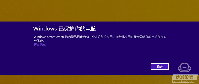
2, TCL TV, enter the settings interface, find the network settings; 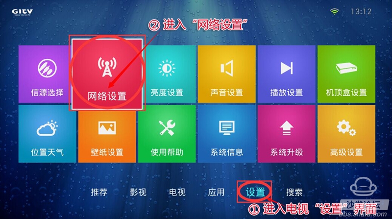
3, using a wireless connection (WIFI) as an example, view the IP address: In the network settings, find the connection on the SSID signal name, press OK; ![]()
4. Record the displayed IP address. 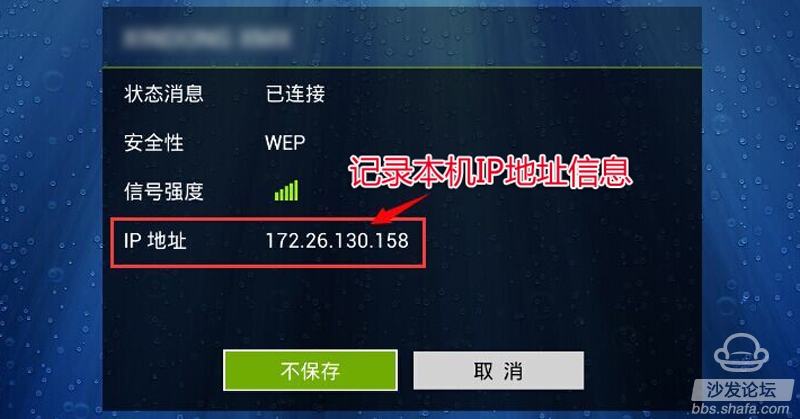
5. Decompress the "TV Application Universal Installer v1.1.1" file package on the computer and double-click to execute it; 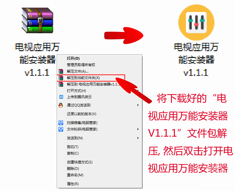
6, run "TV application universal installer v1.1.1", enter the recorded TV IP in the address box, according to start the installation; 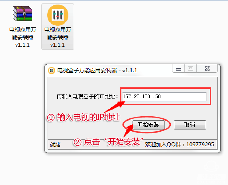
7, "TV Universal App Installer v1.1.1" will automatically connect and install the sofa butler to your TV, please wait a few minutes, as shown below, for the installation is successful; 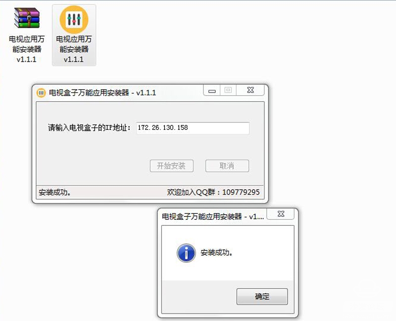

If the installation fails, restart the TV and try again by following the steps.
If you have any questions, please contact us directly. Sofa butler official TCL smart TV exchange QQ group 109779295.
After the sofa butler is installed, you can quickly install all kinds of video, music, games, early education and other applications directly on the TV. The sofa butler → recommendation → TV must have many common applications, such as HDP on-demand, on-demand pudding video.
If this tutorial helps to solve the problem, press Ctrl+D to bookmark this page for your next review. More related tutorials, all at http://
If this tutorial cannot be installed, please click http:// to see more tutorials for installing third-party software on TCL TV LE50D69 .
What PCB designer Must Know About Impedance Control PCB
Controlled Impedance PCB Meaning

Because of complex processors, USB devices and antennas are printed directly on the circuit board surface. The speed of signal switching on the circuit board increases, and the electrical characteristics of the tracks that transmit signals between devices become more and more important. Therefore, more and more PCB designs need impedance control and testing.
When to Use Controlled Impedance
When a signal must have a particular impedance in order to function properly, controlled impedance should be used. In high frequency applications matching the impedance of PCB traces is important in maintaining data integrity and signal clarity. If the impedance of the PCB trace connecting two components does not match the components` characteristic impedance, there may be increased switching times within the device or the circuit. There may also be random errors.
Please note that we also need special instructions here: In DC circuits there is no reactance and the resistance of copper conductors is typically insignificant. However in high speed AC circuits (those with sharp changes in voltage and/or current) the reactance and thus the impedance can become very significant. This can become critical to a design's functionality because of the effects that changes in the impedance along the signals path from transmitter to receiver will have on the efficiency of power transfer as well as signal integrity. While a circuit`s speed is often expressed as the frequency of the wave form: the critical concern is the speed at which the voltage and/or current is required to change.
What Determines Controlled Impedance?
The characteristic impedance of a PCB trace is typically determined by its inductive and capacitive reactance, resistance, and conductance. These factors are a function of the physical dimensions of the trace, the dielectric constant of the PCB substrate material, and dielectric thickness. Typically PCB trace impedance can range from 25 to 125 ohms. The impedance value generated from the PCB structure will be determined by the following factors:
– Width and thickness of the copper signal trace (top and bottom)
– Thickness of the core or prepreg material on either side of the copper trace
– Dielectric constant of the core and prepreg material
– Distance from other copper features
Impedance Control In PCB Design

The Problem: "A", "B" and "C" signals all reach the component at the same time.
The Solution: Apply Impedance to Circuit "C" to slow the signal enough for the component to first calculate ("A"+B").
Similar with a cable, the signal encounters a change of impedance arising from a change in material or geometry. Part of the signal will be reflected and part transmitted. These reflections are likely to cause aberrations on the signal which may degrade circuit performance (e.g. low gain, noise and random errors). In practice, board designers will specify impedance values and tolerances for board traces and rely on the PCB manufacturer to conform to the specification.
When rise times continue to reduce, inevitability the number of traces requiring impedance control will continue to increase. Where impedance control is needed it is important to control it accurately, calculating it with the most representative cross-section we can create.
Applications of Controlled Impedance
Controlled Impedance should be considered for PCBs used in fast digital applications such as:
– Telecommunications
– Computing 100MHz and above
– High Quality Analog Video
– Signal Processing
– RF Communication
Impedance Control PCB Manufacturing
In order to meet the growing demand of impedance control PCB, PCB manufacturers have invested a lot of money and manpower and material resources in production technology, in order to meet the production requirements of customers.
Due to the difficulty of impedance control PCB production, PCB manufacturers generally require PCB designers or purchasers to provide more detailed information and requirements, such as the type of material required, copper weight and thickness of the board, the number of layers, gerber file, so that the manufacturer can prepare the bill of materials (BOM). Impedance information should be clearly marked in Gerber file. If the necessary information is lacking, even a little key information will make it difficult or impossible for the manufacturer's engineers to know exactly what the customer needs.
Impedance-controlled PCBs are also divided into three different situations:
No Impedance Control: This is a situation where you do not need any extra design elements to ensure correct impedance because you have very loose impedance tolerance. Naturally, this will result in a faster-completed, less expensive board because the manufacturer does not have to include any special measures.
Impedance Watching: What is impedance watching? This is a situation where the designer will outline the impedance control trace and the PCB provider adjusts the trace width and dielectric height accordingly. Once the manufacturer approves these specifications, they can begin to manufacture the board. You can request a Time Domain Reflectometry (TDR) test to confirm the impedance for a fee.
Impedance Control: Actual impedance control is something you will typically only request when your design has tight impedance tolerances that could be tough to hit the first time around. When the capability limits of the manufacturer get close to the dimension requirements, it can be tough to ensure target impedance on the initial attempt.
In the case of impedance control, the manufacturer makes the circuit board achieve the target impedance as far as possible. Then they tested TDR to see if they succeeded. If not, they adjust accordingly and try again until they reach the required impedance.
Impedance Control PCB Fabricator
TCL TV LE50D69 how to install third-party applications, TCL TV LE50D69 how to install APK software, TCL TV LE50D69 how to install sofa butler TV application market, a key to download and install on-demand software such as APk?
December 06, 2020