Circuit Design of Wireless Transceiver System for Automotive TPMS System
The current Tire Pressure Monitoring System (TPMS) is primarily divided into two main types: indirect and direct. The direct TPMS system, while widely used, faces challenges such as inaccurate alarm detection and interference from electromagnetic waves and magnetic fields generated by the hub during wireless transmission. To address these issues, this paper introduces a circuit design and solution for a wireless transceiver system in automotive TPMS, based on the RF chip produced by Nordic. This approach enhances the performance and reliability of the direct TPMS system.
In recent years, wireless data transmission technology has become an essential component of small-scale industrial monitoring systems. Compared to traditional wired solutions, wireless data transmission in industrial monitoring typically relies on Radio Frequency (RF) technology to send and receive data packets. Since the entire system is designed specifically for wireless communication, the software development focuses heavily on the RF module, which is the core part of the system. RF refers to high-frequency alternating current that generates electromagnetic waves. Currents with fewer than 1,000 cycles per second are considered low frequency, while those with over 10,000 cycles are classified as high frequency. RF technology plays a crucial role in wireless communication due to its efficiency and broad application range.
1 TPMS System Design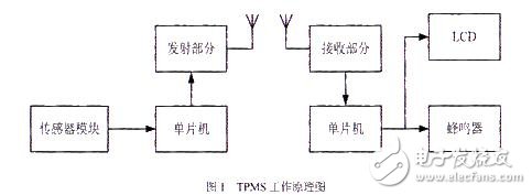
The TPMS system described here operates by transmitting and receiving RF-related information. In the tire section, there are mainly a pressure detection module and an RF transmission module. On the driver side, the system includes an RF reception module and a display alarm module.
The pressure detection module continuously monitors the tire pressure and stores the data on the central processor for later transmission. Once the RF transmission module sends the data, the RF receiver processes it and displays the results on an LCD screen. It also checks the data's validity and triggers an alarm through a buzzer if the tire pressure falls outside the acceptable range. A detailed working principle is illustrated in Figure 1.
2 Comparison and Selection of Wireless Transceiver ChipsWith a wide variety of wireless transceiver chips available, selecting the right one is critical in the design process. The correct choice can significantly reduce development complexity, shorten the project timeline, lower costs, and help bring the product to market faster. When choosing a wireless transceiver chip, several factors must be considered, including power consumption, transmit power, receive sensitivity, the number of peripheral components required, chip cost, and whether Manchester encoding is needed for data transmission.
Key performance indicators for evaluating wireless data transmission and reception include receive sensitivity, dynamic range, selectivity, frequency stability, transmit power, efficiency, frequency range, and power consumption. Below is a comparison of three popular wireless transceiver chips currently on the market, as shown in Table 1.

Based on the data in Table 1 and technical specifications, a transceiver chip that supports a wider frequency band, higher sensitivity, lower receive current under similar conditions, higher transmit current, and fewer peripheral components is more versatile and adaptable to various scenarios.
Considering all these factors, the nRF905 stands out as a superior choice, making it the most suitable option for this design.
3 Introduction to nRF905The nRF905 is a monolithic wireless transceiver chip developed by Nordic Semiconductor. It operates across the 433 MHz, 868 MHz, and 915 MHz ISM bands, eliminating the need for strict frequency restrictions. The nRF905 integrates a complete power management system, frequency synthesizer, modulator, receiver, power amplifier, crystal oscillator, and voltage regulator. It features ShockBurst technology, which automatically handles the preamble and CRC checksum in each packet. The configuration of the nRF905 can be easily programmed via an SPI interface. With low power consumption, it draws only 11 mA in transmit mode at -10 dBm output power and 12.5 mA in receive mode. In Power Down mode, it consumes even less energy, making it ideal for battery-powered applications.
3.1 nRF905 Control ModesThe nRF905 supports two active modes and two power-saving modes. The active modes are ShockBurst RX (receive) and ShockBurst TX (transmit). The power-saving modes include PowerDown, DSP I-programming PowerDown, Standby, and SPI-programming Standby. The specific control mode is determined by the settings of TRX_CE, TX_EN, and PWR, as listed in Table 2.
3.2 Connection Between MCU and nRF905The nRF905 communicates with the microcontroller unit (MCU) through an SPI interface, with the communication speed dependent on the MCU’s interface settings. In receive mode, the address match (AM) and data ready (DR) signals inform the MCU that a valid address and data packet have been received, allowing the MCU to read the data via SPI. In transmit mode, the wireless module automatically generates a preamble and CRC checksum, and the DR signal notifies the MCU that the transmission is complete.
Function description
The socket is ordinary converter,with two output 5V2A power USB power supply at the same time,can be very convenient in use electrical appliances and recharge the equipment at the same time,such as digital products like Iphone Ipad,MP3,MP4 etc.The charge apply to full range of international AC output,no-load power consumption less than 0.3W,with short circuit,overload,over-voltage protection,can be convenient for your life and save more energy
Timer Control Time Adgustment
1.Press the power switch 1 time,the 1HOUR LED will light on.The Timer into ON mode,USB and control socket output ON .
2.Continuously press the power switch the LED light on,the Countdown mode and LED light on will cycle change from 1HR,2HR,4HR,6HR,8HR,10HR.
3.Choose you need countdown time mode,the mode LED will lighto on,start countdown until countdown time finish,the control output and USB change to OFF
4.Then the countdown is start,The Time indicate LED will from high to low auto change until Countdown finish off.
Failure analysis:
1.check whether the power supply connection is good
2.check whether the USB cable is loosen
Warning Note:
1.Use indoor and dry location ONLY
2.The load max does not exceed 15A 3600W
3.This product does not convert voltage please do not miss use DO NOT exceed the maximum loading of 3600 Watts 15A
4.Always have earth connection for safety reason
5.If in doubt please consult with a qualified electrician
USB countdown timer, USB countdown timer socket, USB timer, USB charger timer, USB timer socket
NINGBO COWELL ELECTRONICS & TECHNOLOGY CO., LTD , https://www.cowellsocket.com