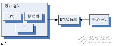
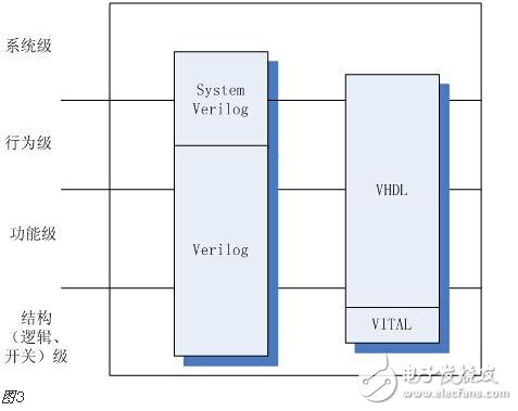
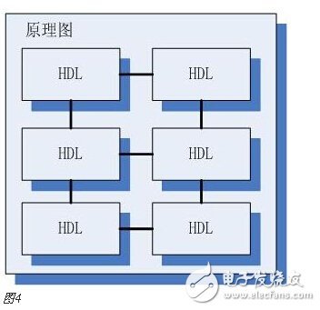
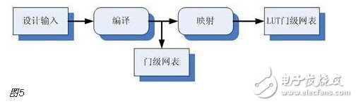
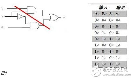
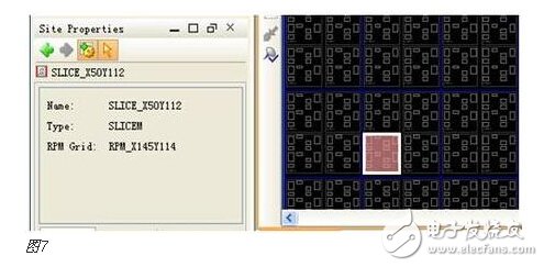
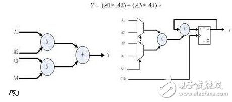
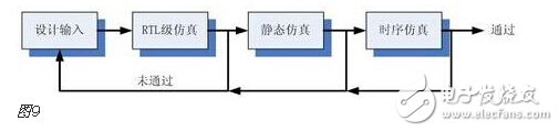
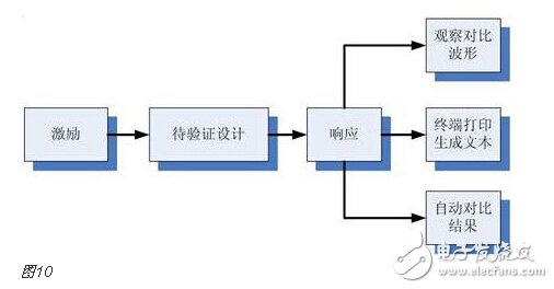
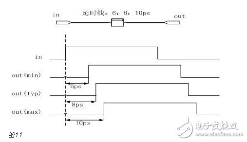
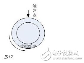
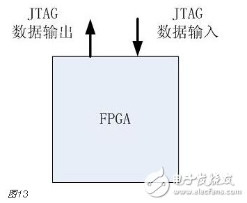
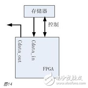
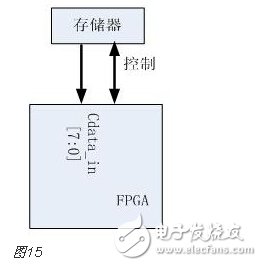
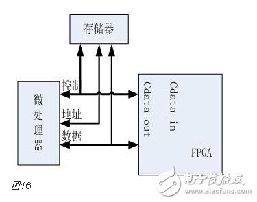
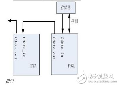
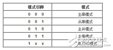
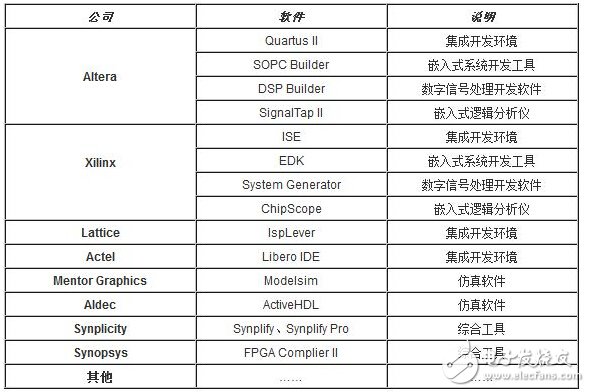
You must know that you have to do a good job, no matter what technology or procedures, it is very important to understand the process of this matter, it determines whether this matter goes smoothly or not. Similarly, let's learn about the technology of FPGA development digital system. Let's start with the specific syntax, tools and tips of the basic programming language using this technology. Let's first understand what the FPGA development process is. The development process of FPGA follows the development process of ASIC. Up to now, the development process of FPGA is generally carried out according to Figure 1. Some steps may be avoided due to the permission of the width of the conditions in the current project. Static simulation process to achieve project time advantage. However, most of the process steps still require us to follow the rules, because the input of these steps is the result of the previous step, and the output is the input relationship of the next step. Such a step is essential. When someone saw this flow chart, the first sigh from the heart was "Ah, how troublesome, especially before the software development turned around. For them, there is very little contact with a technology. So many links to achieve. But this does not explain the specific difficulty of FPGA development, and the software development has input, compilation, linking, and execution steps corresponding to design input, synthesis, place and route, download and write, FPGA development is just to ensure This core realizes the success of each link of the main road plus other modifications (constraints) and verification. Below, we will take the core trunk road as the route, and introduce the physical meaning and achievement goal of each link one by one. Design input The first step of the design input input is separated from the main line in the FPGA development process in Figure 1, and further details are processed. As shown in Figure 2, the design input method has three forms, with IP core. , schematic, HDL, and thus explore the design input method. Schematic input The design of the original digital system circuit may not be imagined. It is built by using a pen and paper logic gate circuit or even a transistor. This way we call the input method of the schematic diagram. At that time, the hardware engineers would sit around and hold the drawings to discuss the circuit. Fortunately, the digital circuit at that time is not very complicated. If it is put into today, a slightly larger system can be regarded as a huge project. If there is a slight circuit to be modified, then you must be an impatient or an acute person. It may lose interest in this field. Having said that, the old engineers who came out in those days, the circuit foundation is really solid. Things always move in the right direction. Later, with the emergence of large computers, engineers began to apply the most primitive punching programming methods to digital circuit design to record the circuit design of our hand-painting. Later, the storage device also began. Used up, from the card to the storage of text files, at that time the netlist file is roughly from that time. The problem to be noted is the relationship between the schematic diagram and the netlist file. The schematic diagram is an input method that we are most convenient for us to design. The netlist file is the computer to transfer the schematic information to the next process or to the simulation platform. Describe the simulation. The design input method is different, but for functional simulation, the final progress to the simulation core should be the same file, then this file is the netlist file. With the aid of computers, the digital circuit design can be said to have improved a lot, but if it is still based on logic gate transistors, it is still cumbersome. Later, the symbol library appeared. The library contains some commonly used devices, such as D flip-flops, and these symbol libraries are constantly enriched as the requirements evolve. Corresponding to the use of these symbol library construction circuits in the schematic diagram, the description of the netlist file obtained by the schematic diagram is also extended accordingly, then the description of the circuit symbols in the netlist file is the initial primitive. It is. As the most primitive digital circuit ASIC design input method, and from the ASIC design flow to the FPGA design process, it has its inherent advantages, that is, intuitive, concise, so that it is still in use. However, it should be noted that this is also relative. For the specific discussion, see the next section. The full name of HDL is the hardware description language Hardware DescripTIon Language. This input method is traced back to the early 1990s. At that time, the scale of the digital circuit was enough to make the door-level abstract design according to the input method at that time, and the left-handedness could not be ignored. It was easy to make mistakes when accidentally, and it was necessary to carry out multi-level schematic cutting. The most important thing is how to do it. To describe digital circuits at a more abstract level. So some EDAs began to provide a textual, very rigorous, error-prone HDL input method that was initially available. Especially in 1980, the US military launched the Very-High-Speed ​​Integrated Circuit program, which is designed to develop the efficiency of digital circuits in large-scale demand in the military. Then this VHSIC hardware The description language is our current VHDL language, and it is also the first standard to become a hardware description language. In contrast, Verilog, which was initiated by the private sector at a later date, was introduced in 1995, and its first version of the IEEE standard was introduced, but it is still in use today. As mentioned earlier, the HDL language has different levels of abstraction. These abstraction layers have switch level, logic level, RTL level, behavior level and system level, as shown in Figure 3. Among them, the switch level and the logic gate level are also called the structure level, which directly reflects the structural characteristics. A large number of primitives are used to call, which is similar to the initial schematic diagram converted into a gate-level netlist. The RTL level can also be called a functional level. In addition to the two mentioned above, the HDL language has also appeared in other HDL languages, including ABEL, AHDL, hardware C (System C language, Handle-C), and System verilog. Among them, ABEL and AHDL are early languages, because they are more or less fatal and are used in a small range or directly eliminated compared to the previous two languages. Because VHDL and Verilog have long simulation defects in the simulation, System verilog and hardware C language are generated. From Figure 3, System Verilog complements Verilog at the system level and behavior level, and is generated by hardware C language. The reason is that there is a desire to integrate software and hardware design into a platform. What is an IP core? Any module that implements a certain function is called IP (Intellectual Property). Here, the IP core is listed separately as an input method, mainly considering that it is possible to form a project by completely using the IP core. Its production can be said to be such a reverse process. As the scale of digital circuits continues to expand, in the face of a super-large project, engineers may reach a consensus to separate the functions of this large-scale and complex design that are often used for certain versatility. Can be used for other designs. When the next design, I found that these assembled modules with certain functions are really easy to use, so more and more such modules with certain functions are extracted, even between engineers to exchange, slowly everyone Noting its intellectual property, so something called IP intellectual property came out, so a new field of integrated circuits (IP design) was born. IP can be divided into three categories according to different sources. The first one is the internal creation module from the previous design, the second is the FPGA manufacturer, and the third is from the IP vendor; the latter two are our concern, this is us. For the existing resource problems considered in the zero development, the cost problem is first solved. The development of the IP method is very beneficial to the project cycle. This is also the reason for displaying the IP resources of the relevant FPGA manufacturers in the FPGA application field. FPGA vendors and IP vendors can provide us with IP at different times during FPGA development. For the time being, we know that they are unencrypted RTL-level IP, encrypted RTL-level IP, unlayed netlist-level IP, and netlist-level IP after place and route. Their meaning is to introduce the development steps of FPGAs in the future, I believe everyone can suddenly realize. It should be noted that the more the IP provided by the FPGA in the front-end step, the better its secondary development, but its performance may be a reverse process, and at the same time more expensive, after all, any provider does not want to The source code program is provided to the other, but in order not to let the customer go to other businesses, it can only increase the price, and at the same time add some legal agreement protection. So the more the back end of the FPGA development step, the opposite is the case, the more the back end, the IP core will be further optimized, the better the performance, but some customers do not want to function. FPGA vendors provide commonly used IP cores. After all, in order to let everyone use their chips, some IP cores with special needs still need to pay. Of course, what needs to be explained here is that the IP of the FPGA manufacturer is rarely used interchangeably. It is easy to think that the manufacturer will not do this to provide services to competitors. IP vendors generally offer unencrypted RTL-level source code at a high price. Sometimes, in order to expand the chip market share, FPGA vendors will purchase third-party IP for further processing and freely submit it to the FPGA chip user. In the above we introduced three input methods. In some places, we will talk about the fourth input method, which is the form of gate-level netlist file input. We do not classify it as an input method here. The generation of the level netlist file is also derived from one of the three input methods introduced or a mixture of several. So there is no classification here. Well, based on the above three input methods, let's explore this dazzling input method. The purpose of the discussion is to let us use them better. First of all, to summarize the advantages and disadvantages of the three, in fact, two, because the IP core regardless of the level, or in the schematic form is instantiated in the form of symbols, or in the HDL by the module instantiation. So here we focus on the advantages and disadvantages of schematics and HDL. The advantage of the schematic diagram is the structural intuition. The advantages of HDL are rigor, support for a wide range of abstract description levels, easy portability, convenient simulation debugging, etc. The disadvantage is that it does not have the advantages of the other party. When HDL appeared, people really thought that the schematic should be taken out of the historical stage, but it still exists until now. Existence is justified. If you exist, you have to use it, but you have to use HDL, so there is a form of mixed programming. In addition to the schematics for the top-level modules, all other internal sub-modules are described using HDL. The modules described by HDL can be converted into symbols by tools and then referenced in the top-level module, which completes the mixed programming. Many beginners who are in contact with many FPGAs are easily confused by the input method of the schematic, and even the deep love, coupled with the cumbersome input aversion of other input methods, is even more in love. When the beginning of the mandatory requirement to develop the habit of using HDL input, some even have the pain of suffering, but as the study progresses, the things are getting bigger and bigger, and taste the sweetness brought by the HDL input method. At that time, I will feel that the bitterness is not eaten. I think that the schematic input method will appear from the current clues that it will end in service in the future. The first is to find a replacement for the schematic itself, that is, the synthesizer and the third-party synthesizer in the mainstream FPGA integrated environment have the RTL view generation function. This view fully shows the structure of the project and can be layered up and down. The biggest advantage is that you can check and verify the integrated circuit condition of the written RTL level code. Another clue is that Modelsim, which is used by everyone, does not provide support for schematic input. The design of the schematic must be converted into RTL-level code or integrated into a netlist form for simulation. Trivial things. The departure of the schematic is only a matter of time. As for which of the current HDL choices is better, this issue is discussed in the place where the basic grammar knowledge of HDL is started. What I want to explain here is that we are not using Verilog to negate other HDL languages. The various HDL disputes have never stopped. There are still four developers, the first one is Verilog/System Verilog, the second is VHDL, and the third is System C. The fourth type is a mixed type of person. In the end, it may be a matter of time. Time proves everything. Comprehensive Whether you use a single input method or a mixed programming (this will be encountered in many cross-company cooperation projects, maybe company A uses VHDL, company B uses Verilog, then it is very likely in this project) With hybrids, we collectively refer to the design input and have to get a description of the design input that matches the FPGA hardware resources. Assuming the FPGA is based on the LUT structure, then we get a gate-level netlist based on the LUT structure. In this process, it can be divided into two steps as shown in the figure. It should be noted that in Altera's development process, the compilation and mapping process is synthesized according to the combination of our description. In the Xilinx development process, the process of obtaining the gate-level netlist from the design input is called synthesis, and the mapping process comes down to it. It is called a substep of the implementation. But the overall process still follows this order, but the name is different from the external ones. The schematic diagram, HDL, and IP core will all generate the gate-level netlist after compilation. The process of generating the gate-level netlist is actually the step of getting up early ASIC, and directly generates the gate netlist. At this time, the netlist file has nothing to do with the specific device. That is to say, the generated gate netlist is also a medium for platform porting. After compiling to get a gate-level netlist, it is different from the masking of the gate-level netlist in the previous ASIC development process. Then we have to consider how to combine with the hardware platform we choose. After all, we use The hardware platform is composed of one LUT (assuming such an FPGA). Then the process of this combination is the mapping process. This process is actually very complicated. First, the formed netlist logic gates need to be planned into small combinations, and then mapped to the LUT. In this process, the planning is carried out according to certain algorithms and regulations. Different algorithms and statutes will get different mappings. Different mappings will provide different choices for later processes, and eventually generate circuits with different performance. Let's take an example of a two-way multiplexer based on SRAM technology. As shown in Figure 6, the two-way multiplexer can be completely split into two sides according to the red line. The original one can be planned to other. In the contents of two tables or tables, since the two parts that are formed can be separately formed into a table, they can also be planned into a table formed by other circuits. The mapping project is more complicated and the amount of computation is also large. It is also a problem that has always existed in the FPGA development process. The time to form the final configurable binary file is very long, especially for some larger projects, which consume a long time. One point is the mapping, and the specific mapping algorithm is beyond the scope of the book. It is emphasized that the mapping is related to the device. Even in the same series, the internals of different models are different. It is like a unit in a unit building, but in each unit. Decoration, furniture, etc. are all different. Place and route Speaking of this one, there is just one example to explain this concept. Recently, North Korea is expected to rent hundreds of thousands of hectares of land in the Russian Far East to cultivate agricultural products. I will first open the success of future purchases, assuming success, and with the variety and quantity of crops that I hope to cultivate, there are all kinds of vegetables, staple foods, poultry farms, fruit trees and so on. The LUT gate-level netlists that we have done in the previous process are like this list. After obtaining such a list, we assume that there is a certain distribution of sunshine, water resources and temperature difference on the 100,000 hectares of land. Everyone knows that the growth and high yield of crops are related to Yangguan, or related to water resources, or related to temperature difference, and the livestock materials of poultry are related to crop by-products. So the next thing to do is to rationally layout according to the existing natural conditions and the required environmental characteristics of the agricultural products, and which places are suitable for what to do. Soon after we return to FPGA development, the list we got through the previous steps is the LUT gate-level netlist. The only thing provided in the netlist is the connection of some LUT structures from the logical relationship. We need to configure these LUT structures to the specific location of the FPGA. It should be noted that any hardware structure in the FPGA is calibrated according to the horizontal and vertical coordinates. The selected one is SLICE. The SLICE stores the table and other structures. Its position is on X50Y112. The coordinates of different resources are different, but the zeros of the coordinates are common. The problem to be considered in the layout of the FPGA is how to properly put these existing logically connected LUTs and other elements into the existing FPGA to ensure quality when the functional requirements are met. Specifically, for example, a circuit such as a multiplier is suitable for being placed near the RAM. Of course, the hardware layout of the hardware multiplier is generally near the memory, which is advantageous for shortening the delay time of multiplication, and what kind of circuit needs to be configured with high speed and the like. The layout of the 100,000 hectares is well planned, and the agricultural products will have a good harvest. The same FPGA development layout is laid out, and the circuit built by the FPGA will be more stable and expandable. In the last section, we arranged 100,000 hectares of land, and what kind of land should be used. Before the implementation, there are still some things that must be done, such as the irrigation of crops. It is a problem without a good irrigation system. For example, if the harvest is harvested, at this time, the big truck can reach the road junction of each farmland. It is also a problem that needs to be solved. The construction of the irrigation system and the road connecting each piece or related field is like the process of our wiring. We use the layout in the FPGA to know which SLICE the LUTs are specifically distributed to, but on the one hand how to connect these SLICEs, how to make the input signals reach the corresponding starting processing point and how to let the output reach the output IO, and connect The overall performance of the circuit is good, which is what needs to be done in the wiring. To achieve the best wiring, of course, the design of the routing algorithm and many details, such as the routing resources, PLL resource distribution. But these do not have many benefits for us to understand the concept of wiring. For the time being, it is not in-depth, and it is essentially a problem of optimal line. Constraints, as seen in Figure 1, appear in the two process links of synthesis and place and route, we temporarily specify that it is Constraint 1 and Constraint 2, or synthetic constraints and place and route constraints, layout and routing constraints can be divided For position constraints, timing constraints. Constraints are the custom rules for these links. The general development environment has defaults for these constraints. These default settings are still applicable in most cases, but usually the I/O constraints in the placement and routing constraints must be given for each of our projects. At the same time, the development tool opens other constraint interfaces, allowing us to set these rules. What are the specific constraints? How to do this is discussed later when the tools are used. Here we understand the basic concepts of these constraints. I believe that you have subconsciously linked the comprehensive constraints and the integration process. Yes, the comprehensive constraints are actually done in the synthesis process to guide the synthesis process, including compilation and mapping. We already know that the synthesis process is to convert the RTL-level circuit description into a hardware unit (LUT) on the FPGA to form a circuit composed of hardware units that exist in the FPGA. We still use the examples we have shown before, different constraints will lead to the generation of circuits with different performance. To integrate such a completed circuit, the circuit obtained without the resource sharing is shown in the circuit shown on the left side of FIG. 8, and after the constraint of resource sharing is added, the circuit structure obtained is as shown in the circuit on the right side of FIG. Through the previous analysis, the left circuit structure resource consumption is high but the speed is fast, while the right structure consumes less resources, but the speed is slow, and the multiplier needs time division multiplexing. Of course, this is just an example, but it is enough to show that different comprehensive guiding principles are comprehensive constraints, which will produce different circuits. When the obtained circuit performance cannot meet the demand, the comprehensive constraint is appropriately considered to achieve the effect of a speed and area conversion, and the performance is improved. The speed and area of ​​circuit implementation are two contradictory problems throughout the FPGA development process. The comprehensive constraint is one of the ways to achieve speed and face balance movement in a small range. That's right, you think right again. Positional constraints are related to our layout. It refers to the layout strategy. The layout of our existing hardware resources is chosen according to the selected FPGA platform. The most typical location constraint is the I/O constraint. A typical system has both input and output, regardless of whether it is an input or an output, and is an endpoint from the I/O. From which endpoint the input comes in, from which endpoint the output goes, the input is the endpoint that needs to support what electrical characteristics, and the output is what electrical specific endpoints need to be supported. These are all things that I/O constraints do. Any project must have such a constraint. Another typical location constraint is the physical definition involved in incremental compilation. The advent of incremental compilation was due to the long time-consuming nature of synthesis and place and route during FPGA development. The idea is to cut the FPGA into a number of small blocks of FPGA, and then agree which specific small FPGA to place what module, what kind of function to achieve, physically defined. When the project is modified, the development platform will detect which small FPGAs have not been modified and which have been modified, and then re-synthesize the modified portions. In this way, compared with the original modification, the whole project re-passed those processes, and the time was saved. It is estimated that there is not much suspense, and timing constraints are largely related to wiring. Why do you want to do this constraint? Since the signal is transmitted on-chip on one hand, it takes time. On the other hand, a large number of registers have reaction time, and these times are idealized at the beginning of our development. But considering the real situation, if the running speed is relatively high, it reaches a speed of 200M. Of course, this high speed is related to a specific chip. The high-performance chip itself can run at a high speed, and the 200M is relatively high speed. For some low-performance chips, it may not reach 200M. At this time, when these times reach the same level of system time, it is likely to affect the performance of the circuit. At some point, the incoming signal does not come. By default, the error signal is collected. In order to make the delay time brought by these hardwares more ideal, we need to optimize these factors that determine the time delay to reduce the time delay. For the factor of the response time of the register itself, our developers are powerless. The optimization we have to do is the wiring. Whether it is a straight line or other, not only depends on its own path, but also related to the entire system wiring, like the bucket principle, the system performance is determined by the worst path delay. Timing constraints do these things, but timing constraints do not refer to the specific connection of each line. This work is implemented by software just like the previous processes. It is wired by the software itself and then analyzed. If we do not meet the timing requirements, we will make some guidance and constraints on the specific problem path. The addition of timing constraints mainly includes periodic constraints, input offset constraints, and output offset constraints. The specific process will be followed by specific hands-on guidance in the following sections. After the introduction from design input to synthesis to place and route process, let's focus on the corresponding simulations involved in these processes. Simulation, literally speaking, simulates the real situation. The simulation in our FPGA design is to simulate the condition of the real circuit and see if the circuit is the one we need. If we consider FPGA development to form a circuit as a production process, then the three simulations (RTL-level simulation, static simulation, and timing simulation) contained in the FPGA development process are like three test stations in the product line. As shown in Figure 9, any of the three processes has a problem. After modifying the design, you have to go back to the three cards, so try to find the problem at the source. The so-called testbench, the test platform, in detail, is to add incentives to the design to be verified, and observe whether the output response meets the design requirements. Test platform, the test platform needs to be used in functional simulation, static simulation and timing simulation. At the beginning, for some beginners, there are some simple things that are encountered. The test platform is also very simple. The test structure can be clearly presented with a single file. For some complex projects, the test is not so simple, so it is also dedicated to an industry - the test industry. At this time we need to use a concept is structured testing. A complete test platform is shown in Figure 10, which is composed of sub-structures. The judgment of the design test results can be obtained not only by observing the contrast waveform, but also by using script commands to print useful output information to the terminal or generate text. To observe, you can also write a piece of code to let them automatically compare the output. The test platform is designed in a variety of ways, and can use flexible Verilog verification scripts, but it is also a language based on hardware language but also for software testing. Sometimes it is parallel and sometimes sequential. Only by mastering these key points can the service test be well served. One point to note is that whether you are already using Verilog to write a test platform or just learning to write a test platform, then it is recommended that you can still use the new Verilog syntax in System Verilog or try it out. System Verilog is a trend. It is itself a backward compatible third generation Verilog. Here RTL level simulation belongs to the first test, and some occasions are called function simulation. In order to highlight the difference between the static simulation and the latter static simulation, we will make it very big when we introduce static simulation later. We still call it this way. It tests the description of the project at the register transfer level to see the correctness of the functions it implements at the RTL level. Regarding RTL level simulation, if the design is designed to input to the schematic, it is not supported in some simulation tools, such as Modelsim. At this time, functional verification is required, and the schematic can be converted into HDL description, or directly After the project is converted into a LUT gate level netlist, the static simulation to be described later is completed. Verification of all logic functions is expected to be done at the RTL level, and the problem is found in the RTL-level simulation process as much as possible, reducing the iterations caused by the problems found later. Static simulation, in some places, the nickname is gate-level simulation, which should be the integrated LUT gate-level netlist. It is a simulation done after the integration process. Some development platforms divide static simulation into compilation simulation and mapping simulation. For example, ISE does this, but personally feel that there should be very few occasions to do this compilation simulation. The purpose of the static simulation is to verify that the correctness of the verification project is checked functionally when the project is described by the LUT gate level netlist. Both Altera and Xilinx development platforms directly support static simulation, but because the simulators of their respective manufacturers are not professional, we still use third-party simulation tools. At this time, the input under the third-party tool must be a LUT gate-level netlist file that is integrated by the comprehensive tool and covers all the information of the project. The general professional third-party integrated tools do not have comprehensive functions. At least when we use Modelsim, we do not ask us to add the specific FPGA information of the project. This is also the basis for static simulation of the gate-level simulation of the LUT gate-level netlist. Timing simulation is done after place and route. When we introduced timing constraints in the previous section, timing constraints can be made when the routing delay problem affects the performance of the circuit. Then the acquisition of this delay problem can be obtained through timing simulation, and of course there is an overload condition that is delayed, which is the static timing analysis described in the following section. Under normal circumstances, after the circuit completes the routing process, it will generate a delay information file, which is referred to as SDF (standrad dealy format) file, and the Quartus platform exists in the form of .sdo file. There are three types of delay information, which are minimum value, typical value, and maximum value. The existing form is the minimum value: typical value: maximum value, and the general abbreviation min:typ:max. It also shows that the delay information in the FPGA can not be accurately obtained, only the approximation, because in the same device, the logic gates of different regions are also likely to be the same kind of logic gates in other regions. The delay is not the same. Here is an example to illustrate the meaning of these three values. As shown in the above figure, this is a delay information describing a delay line. The delay information is sent from the in endpoint to the out endpoint. After the input transition occurs, the signal transition is transmitted to the minimum, the typical value and the maximum value respectively. Out endpoint. We are just a delay line here. There is also a kind of delay information in the delay information file, which is some cell delay with logic function. At this time, the signal transition is divided into high to low and low to high because The three kinds of delay values ​​of these two kinds of jumps in these devices are different, and they have to be discussed separately, and they are analogized in a certain case. In the post-simulation, it is only necessary to add the delay information of the wiring after the static simulation is completed, and then analyze whether the logic function satisfies the requirements. The platform usage of the post-guideline is the same as before. Generally, third-party simulation tools are used, typically Modlesim. For the specific operation process, see the software-related operation chapter. Static timing analysis, referred to as STA (StaTIc TIming Analysis), this process is done before the simulation. After the place and route, a timing analysis report is generated, which is accurately calculated by the analysis tool after extracting the parasitic parameters from the routing power of the wiring. In this report, some key paths are suggested. The so-called key road strength refers to the signal node flow with prominent delay information. The analysis can obtain the path that does not meet the timing requirements. This process is the STA process. The characteristic of static timing analysis is that it can exhaust all paths without input vector, and it runs fast and takes up less memory. It can not only perform comprehensive timing function check on chip design, but also optimize the result of timing analysis. design. Many designs can be based on the success of functional verification, plus a good static timing analysis, can replace the very long post-simulation, which is a very reliable simplification process. Post-simulation also has logic verification for static timing analysis, and analyzes the logic based on the added delay information. Online debugging is also called board level debugging. It is the case where the code is run after the project is downloaded to the FPGA chip. Some people will think that we have not done simulation, even the timing simulation has passed, there will be problems? In practice, there are some situations where we need to use online debugging: FPGA design errors that are not comprehensive and not found. In many cases, due to the complexity, 100% code coverage is not possible; In the board-level interaction, there are asynchronous events, it is difficult to do simulation, or the simulation takes a long time to run; In addition to the FPGA itself, there may be problems with on-board interconnect reliability, power problems, and signal interference between ICs, which may cause system operation errors; There are two main ways to debug online. One is to use an external test device to transmit internal signals to the FPGA pins, and then use an oscilloscope or logic analyzer to observe the signal. The other is to use an embedded logic analyzer in the design.æ’入逻辑分æžä»ªï¼Œåˆ©ç”¨JTAG边缘数æ®æ‰«æ和开å‘工具完æˆæ•°æ®äº¤äº’。 嵌入å¼é€»è¾‘分æžä»ªçš„原ç†ç›¸å½“与在FPGAä¸å¼€è¾Ÿä¸€ä¸ªçŽ¯å½¢å˜å‚¨å™¨ï¼Œå˜å‚¨å™¨çš„大å°å†³å®šäº†èƒ½å¤ŸæŸ¥çœ‹çš„æ•°æ®çš„深度,是å¯ä»¥äººä¸ºè®¾å®šçš„,但是ä¸å¾—超出资æºã€‚在FPGAå†…éƒ¨ï¼Œæ ¹æ®è®¾ç½®çš„需è¦æŸ¥çœ‹çš„ä¿¡å·èŠ‚点信æ¯å’Œé©±åŠ¨çš„é‡‡æ ·æ—¶é’Ÿï¼Œå¯¹ä¿¡æ¯è¿›è¡Œé‡‡æ ·ï¼Œå¹¶æ”¾ç½®åˆ°è®¾å®šçš„å˜å‚¨ç©ºé—´é‡Œï¼Œå˜å‚¨ç©ºé—´æ˜¯çŽ¯å½¢çš„,内容éšæ—¶é—´æ›´æ–°ã€‚然åŽé€šè¿‡åˆ¤æ–触å‘点æ¥æ£€æŸ¥é‡‡é›†æ•°æ®ï¼Œä¸€æ—¦æ»¡è¶³è§¦å‘æ¡ä»¶ï¼Œè¿™ä¸ªæ—¶å€™ä¼šåœæ¢æ‰«æ,然åŽå°†è§¦å‘点å‰åŽçš„一些数æ®è¿”回给PC端的测试工具进行波形显示,供开å‘者进行调试。 ç›®å‰çš„调试工具都是和本身的FPGAå¼€å‘å¹³å°æŒ‚钩的,ä¸åŒFPGA厂商都会有开å‘软件平å°ï¼ŒåµŒå…¥å¼é€»è¾‘分æžä»ªä¹Ÿå°±ä¸åŒã€‚Altera 厂家æ供的是SignalTapII,而Xilinx厂家æ供的是ChipScope,这些工具的具体使用在åŽé¢å·¥å…·ä¸è¯¦è§£ã€‚ 当然这里除了嵌入å¼é€»è¾‘分æžä»ªå¤–,å„厂家还æ供了一些其他的在线调试工具,例如SignalProbeç‰ç‰ï¼Œä½†æ˜¯æˆ–多或少的用的人ä¸æ˜¯å¾ˆå¤šï¼Œæœ‰å…´è¶£çš„å¯ä»¥æ‰¾åˆ°è¯¥åŠŸèƒ½ä½¿ç”¨çš„说明手册。 好了,到了我们最åŽä¸€ä¸ªçŽ¯èŠ‚å°±å¯ä»¥å®ŒæˆFPGAçš„æµç¨‹äº†ã€‚这一部分我们分四个å°èŠ‚æ¥è®²ï¼Œé¦–先是针对大家很多人ä¸æ˜¯å¤ªæ¸…楚的FPGAé…置过程安排的,éšåŽä¸€èŠ‚ä¸ºäº†æ›´åŠ æ·±ç†è§£ï¼Œä¸¾äº†altera çš„FPGAå™è¿°é…置全过程,第三å°èŠ‚是探讨FPGA主è¦çš„é…置模å¼ï¼Œæœ€åŽä¸€èŠ‚就是æ£å¯¹è¿™äº›é…置模å¼å±•å¼€çš„对比选择探讨。 在FPGAæ£å¸¸å·¥ä½œæ—¶ï¼Œé…置数æ®å˜å‚¨åœ¨SRAMä¸ï¼Œè¿™ä¸ªSRAMå•å…ƒä¹Ÿè¢«ç§°ä¸ºé…ç½®å˜å‚¨å™¨ï¼ˆconfigure RAM)。由于SRAM是易失性å˜å‚¨å™¨ï¼Œå› æ¤åœ¨FPGA上电之åŽï¼Œå¤–部电路需è¦å°†é…置数æ®é‡æ–°è½½å…¥åˆ°èŠ¯ç‰‡å†…çš„é…ç½®RAMä¸ã€‚在芯片é…置完æˆä¹‹åŽï¼Œå†…部的寄å˜å™¨ä»¥åŠI/O管脚必须进行åˆå§‹åŒ–(iniTIalization),ç‰åˆ°åˆå§‹åŒ–完æˆä»¥åŽï¼ŒèŠ¯ç‰‡æ‰ä¼šæŒ‰ç…§ç”¨æˆ·è®¾è®¡çš„功能æ£å¸¸å·¥ä½œï¼Œå³è¿›å…¥ç”¨æˆ·æ¨¡å¼ã€‚ FPGA上电以åŽé¦–先进入é…置模å¼ï¼ˆconfiguration),在最åŽä¸€ä¸ªé…置数æ®è½½å…¥åˆ°FPGA以åŽï¼Œè¿›å…¥åˆå§‹åŒ–模å¼ï¼ˆinitialization),在åˆå§‹åŒ–完æˆåŽè¿›å…¥ç”¨æˆ·æ¨¡å¼ï¼ˆuser-mode)。在é…置模å¼å’Œåˆå§‹åŒ–模å¼ä¸‹ï¼ŒFPGA的用户I/O处于高阻æ€ï¼ˆæˆ–内部弱上拉状æ€ï¼‰ï¼Œå½“进入用户模å¼ä¸‹ï¼Œç”¨æˆ·I/O就按照用户设计的功能工作。 一个器件完整的é…置过程将ç»åŽ†å¤ä½ã€é…置和åˆå§‹åŒ–ç‰3个过程。FPGAæ£å¸¸ä¸Šç”µåŽï¼Œå½“å…¶nCONFIG管脚被拉低时,器件处于å¤ä½çŠ¶æ€ï¼Œè¿™æ—¶æ‰€æœ‰çš„é…ç½®RAM内容被清空,并且所有I/O处于高阻æ€ï¼ŒFPGA的状æ€ç®¡è„šnSTATUSå’ŒCONFIG_DONE管脚也将输出为低。当FPGAçš„nCONFIG管脚上出现一个从低到高的跳å˜ä»¥åŽï¼Œé…置就开始了,åŒæ—¶èŠ¯ç‰‡è¿˜ä¼šåŽ»é‡‡æ ·é…置模å¼ï¼ˆMSEL)管脚的信å·çŠ¶æ€ï¼Œå†³å®šæŽ¥å—何ç§é…置模å¼ã€‚éšä¹‹ï¼ŒèŠ¯ç‰‡å°†é‡Šæ”¾æ¼æžå¼€è·¯ï¼ˆopen-drain)输出的nSTATUSç®¡è„šï¼Œä½¿å…¶ç”±ç‰‡å¤–çš„ä¸Šæ‹‰ç”µé˜»æ‹‰é«˜ï¼Œè¿™æ ·ï¼Œå°±è¡¨ç¤ºFPGAå¯ä»¥æŽ¥æ”¶é…置数æ®äº†ã€‚在é…置之å‰å’Œé…置过程ä¸ï¼ŒFPGA的用户I/Oå‡å¤„于高阻æ€ã€‚ 在接收é…置数æ®çš„过程ä¸ï¼Œé…置数æ®ç”±DATA管脚é€å…¥ï¼Œè€Œé…置时钟信å·ç”±DCLK管脚é€å…¥ï¼Œé…置数æ®åœ¨DCLK的上å‡æ²¿è¢«é”å˜åˆ°FPGAä¸ï¼Œå½“é…置数æ®è¢«å…¨éƒ¨è½½å…¥åˆ°FPGAä¸ä»¥åŽï¼ŒFPGA上的CONF_DONEä¿¡å·å°±ä¼šè¢«é‡Šæ”¾ï¼Œè€Œæ¼æžå¼€è·¯è¾“出的CONF_DONEä¿¡å·åŒæ ·å°†ç”±å¤–éƒ¨çš„ä¸Šæ‹‰ç”µé˜»æ‹‰é«˜ã€‚å› æ¤ï¼ŒCONF_DONE管脚的从低到高的跳å˜æ„味ç€é…置的完æˆï¼Œåˆå§‹åŒ–过程的开始,而并ä¸æ˜¯èŠ¯ç‰‡å¼€å§‹æ£å¸¸å·¥ä½œã€‚ INIT_DONE是åˆå§‹åŒ–完æˆçš„指示信å·ï¼Œå®ƒæ˜¯FPGAä¸å¯é€‰çš„ä¿¡å·ï¼Œéœ€è¦é€šè¿‡Quartus II工具ä¸çš„设置决定是å¦ä½¿ç”¨è¯¥ç®¡è„šã€‚在åˆå§‹åŒ–过程ä¸ï¼Œå†…部逻辑ã€å†…部寄å˜å™¨å’ŒI/O寄å˜å™¨å°†è¢«åˆå§‹åŒ–,I/O驱动器将被使能。当åˆå§‹åŒ–完æˆä»¥åŽï¼Œå™¨ä»¶ä¸Šæ¼æžå¼€å§‹è¾“出的INIT_DONE管脚被释放,åŒæ—¶è¢«å¤–部的上拉电阻拉高。这时,FPGA完全进入用户模å¼ï¼Œæ‰€æœ‰çš„内部逻辑以åŠI/O都按照用户的设计è¿è¡Œï¼Œè¿™æ—¶ï¼Œé‚£äº›FPGAé…置过程ä¸çš„I/O弱上拉将ä¸å¤å˜åœ¨ã€‚ä¸è¿‡ï¼Œè¿˜æœ‰ä¸€äº›å™¨ä»¶åœ¨ç”¨æˆ·æ¨¡å¼ä¸‹I/O也有å¯ç¼–程的弱上拉电阻。在完æˆé…置以åŽï¼ŒDCLKä¿¡å·å’ŒDATA管脚ä¸åº”该被浮空(floating),而应该被拉æˆå›ºå®šç”µå¹³ï¼Œé«˜æˆ–低都å¯ä»¥ã€‚ 如果需è¦é‡æ–°é…ç½®FPGA,就需è¦åœ¨å¤–部将nCONFIGé‡æ–°æ‹‰ä½Žä¸€æ®µæ—¶é—´ï¼Œç„¶åŽå†æ‹‰é«˜ã€‚当nCONFIG被拉低å¼ï¼ŒnSTATUSå’ŒCONF_DONE也将éšå³è¢«FPGA芯片拉低,é…ç½®RAM被清,所有I/O都å˜æˆä¸‰æ€ã€‚当nCONFIGå’ŒnSTATUS都å˜ä¸ºé«˜æ—¶ï¼Œé‡æ–°é…置就开始了。 é…ç½®æ¨¡å¼ è¿™ä¸€å—分æˆä¸¤éƒ¨åˆ†ï¼Œä¸€éƒ¨åˆ†æ˜¯åœ¨çº¿è°ƒè¯•é…置,å¦ä¸€å—是固化,å³å°†å·¥ç¨‹é…置到相应å˜å‚¨å•å…ƒä¸ï¼Œä¸Šç”µåŽï¼Œé€šè¿‡å˜å‚¨åœ¨å˜å‚¨å™¨ä¸çš„内容é…ç½®FPGA。 在线é…ç½® 第一部分在线调试é…置过程是通过JTAG模å¼å®Œæˆçš„,如图13所示,在JTAG模å¼ä¸ï¼ŒPCå’ŒFPGA通信的时钟为JTAG接å£çš„TCLK,数æ®ç›´æŽ¥ä»ŽTDI进入FPGA,完æˆç›¸åº”功能的é…置。 JTAG接å£æ˜¯ä¸€ä¸ªä¸šç•Œæ ‡å‡†æŽ¥å£ï¼Œä¸»è¦ç”¨äºŽèŠ¯ç‰‡æµ‹è¯•ç‰åŠŸèƒ½ã€‚FPGA基本上都å¯ä»¥æ”¯æŒJTAG命令æ¥é…ç½®FPGAçš„æ–¹å¼ï¼Œè€Œä¸”JTAGé…置方å¼æ¯”其他任何方å¼ä¼˜å…ˆçº§éƒ½é«˜ã€‚JTAG接å£æœ‰4个必需的信å·TDI, TDO, TMSå’ŒTCK以åŠ1个å¯é€‰ä¿¡å·TRSTæž„æˆï¼Œå…¶ä¸ï¼š TDI,用于测试数æ®çš„输入; TDO,用于测试数æ®çš„输出; TMS,模å¼æŽ§åˆ¶ç®¡è„šï¼Œå†³å®šJTAG电路内部的TAP状æ€æœºçš„è·³å˜ï¼› TCK,测试时钟,其他信å·çº¿éƒ½å¿…须与之åŒæ¥ï¼› TRST,å¯é€‰ï¼Œå¦‚æžœJTAG电路ä¸ç”¨ï¼Œå¯ä»¥è®²å…¶è¿žåˆ°GND。 第二部分固化程åºåˆ°å˜å‚¨å™¨ä¸çš„过程å¯ä»¥åˆ†ä¸ºä¸¤ç§æ–¹å¼ï¼Œä¸»æ¨¡å¼å’Œä»Žæ¨¡å¼ã€‚主模å¼ä¸‹ FPGA器件引导é…ç½®æ“作过程,它控制ç€å¤–部å˜å‚¨å™¨å’Œåˆå§‹åŒ–过程;从模å¼ä¸‹åˆ™ç”±å¤–部计算机或控制器控制é…置过程。主ã€ä»Žæ¨¡å¼ä»Žä¼ 输数æ®å®½åº¦ä¸Šï¼Œåˆåˆ†åˆ«å¯ä»¥åˆ†ä¸ºä¸²è¡Œå’Œå¹¶è¡Œã€‚ (1ï¼‰ä¸»ä¸²æ¨¡å¼ ä¸»ä¸²æ¨¡å¼æ˜¯æœ€ç®€å•çš„固化模å¼ï¼Œå¦‚图14所示,这个模å¼è¿‡ç¨‹ä¸éœ€è¦ä¸ºå¤–部å˜å‚¨å™¨æ供一系列地å€ã€‚它利用简å•çš„脉冲信å·æ¥è¡¨æ˜Žæ•°æ®è¯»å–的开始,接ç€ç”±FPGAæ供给å˜å‚¨å™¨æ—¶é’Ÿï¼Œå˜å‚¨å™¨åœ¨æ—¶é’Ÿé©±åŠ¨ä¸‹ï¼Œå°†æ•°æ®è¾“入到FPGA Cdata_in端å£ã€‚ (2ï¼‰ä¸»å¹¶æ¨¡å¼ ä¸»å¹¶æ¨¡å¼å…¶å®žå’Œä¸»ä¸²æ¨¡å¼çš„ä¸€æ ·æœºç†ï¼Œåªä¸è¿‡æ˜¯åœ¨ä¸»ä¸²çš„基础上,åŒå‘¨æœŸæ•°å†…ä¼ é€çš„æ•°æ®å˜æˆ8ä½ï¼Œæˆ–者更高,如图15ã€‚è¿™æ ·ä¸€æ¥ï¼Œä¸»å¹¶è¡Œç›¸æ¯”主串行的数度è¦ä¼˜å…ˆäº†ã€‚现代有些地方已采用这ç§æ–¹å¼æ¥é…ç½®FPGA的了。 (3ï¼‰ä»Žå¹¶æ¨¡å¼ ä»Žä¸Šé¢çœ‹åˆ°ï¼Œä¸»æ¨¡å¼ä¸‹çš„连接还是很简å•çš„。但是有时候,系统å¯èƒ½ç”¨å…¶ä»–微处ç†å™¨æ¥å¯¹FPGA进行é…置。这里的微处ç†å™¨å¯ä»¥æŒ‡FPGA内嵌的处ç†å™¨ï¼Œæ¯”如说Nios。微处ç†å™¨æŽ§åˆ¶ç€ä½•æ—¶é…ç½®FPGA,从哪读å–é…置文件。如图16,这ç§æ–¹å¼çš„优点是处ç†å™¨å¯ä»¥çµæ´»éšæ—¶å˜æ›´FPGAé…置,åŒæ—¶é…置的速度也快。微处ç†å™¨å…ˆä»Žå¤–部å˜å‚¨è®¾å¤‡é‡Œè¯»å–一个å—节的数,然åŽå†™åˆ°FPGA里。 (4ï¼‰ä»Žä¸²æ¨¡å¼ ç†è§£äº†ä»Žå¹¶æ¨¡å¼ï¼Œä»Žä¸²æ¨¡å¼å°±ä¸ç”¨å¾ˆå¤šè§£é‡Šäº†ï¼Œå®ƒçš„特点就是节约FPGA管脚I/O。 (5ï¼‰å¤šç‰‡çº§è” å¤šç‰‡æ¨¡å¼æœ‰ä¸¤ç§ï¼Œä¸€ç§æ˜¯é‡‡ç”¨èŠèŠ±é“¾çš„æ€æƒ³ï¼Œå¤šç‰‡FPGA共享一个å˜å‚¨å™¨ï¼Œå¦å¤–一个是å¯ä»¥ä½¿ç”¨å…¶ä»–å˜å‚¨å™¨é…ç½®ä¸åŒçš„FPGA。如果所示是一个共享型的结构,显示å¯åŠ¨äº†ã€‚这里分主FPGA和从FPGA,主FPGAå’Œå˜å‚¨å™¨æ˜¯ä½¿ç”¨ä¸²è¡Œä¸»æ¨¡å¼æ¥é…置,而åŽé¢é‚£ä¸ªçš„é…置是通过第一é…置好的FPGA上微处ç†å™¨è¿›è¡Œå调的。 模å¼é€‰æ‹© 现今FPGA应该å¯ä»¥æ”¯æŒä¸Šé¢äº”ç§é…置模å¼ï¼Œæ˜¯é€šè¿‡3个模å¼å¼•è„šæ¥å®žçŽ°çš„ï¼Œå…·ä½“çš„æ˜ å°„å¦‚ä¸‹è¡¨ï¼Œåœ¨ä»ŠåŽæ¨¡å¼è¿˜æ˜¯æœ‰å¯èƒ½å¢žåŠ 的。 在PS模å¼ä¸‹ï¼Œå¦‚æžœä½ ç”¨ç”µç¼†çº¿é…ç½®æ¿ä¸Šçš„FPGA芯片,而这个FPGA芯片已ç»æœ‰é…置芯片在æ¿ä¸Šï¼Œé‚£ä½ 就必须隔离缆线与é…置芯片的信å·ã€‚一般平时调试时ä¸ä¼šæŠŠé…置芯片焊上的,这时候用缆线下载程åºã€‚åªæœ‰åœ¨è°ƒè¯•å®Œæˆä»¥åŽï¼Œæ‰æŠŠç¨‹åºçƒ§åœ¨é…置芯片ä¸ï¼Œ 然åŽå°†èŠ¯ç‰‡ç„Šä¸Šã€‚或者é…置芯片就是å¯ä»¥æ–¹ä¾¿å–下焊上的那ç§ã€‚è¿™æ ·å‡ºäº†é—®é¢˜è¿˜å¯ä»¥æ–¹ä¾¿åœ°è°ƒè¯•ã€‚ . 对FPGA芯片的é…ç½®ä¸ï¼Œå¯ä»¥é‡‡ç”¨AS模å¼çš„方法,如果采用EPCS的芯片,通过一æ¡ä¸‹è½½çº¿è¿›è¡Œçƒ§å†™çš„è¯ï¼Œé‚£ä¹ˆå¼€å§‹çš„“nCONFIG,nSTATUSâ€åº”该上拉,è¦æ˜¯è€ƒè™‘多ç§é…置模å¼ï¼Œå¯ä»¥é‡‡ç”¨è·³çº¿è®¾è®¡ã€‚让é…置方å¼åœ¨è·³çº¿ä¸åˆ‡æ¢ï¼Œä¸Šæ‹‰ç”µé˜»çš„阻值å¯ä»¥é‡‡ç”¨10K一般在åšFPGA实验æ¿çš„时候,用AS+JTAGæ–¹å¼ï¼Œè¿™æ ·å¯ä»¥ç”¨JTAGæ–¹å¼è°ƒè¯•ï¼Œè€Œæœ€åŽç¨‹åºå·²ç»è°ƒè¯•æ— 误了åŽï¼Œå†ç”¨AS模å¼æŠŠç¨‹åºçƒ§åˆ°é…置芯片里去。 在围绕图1把FPGAå¼€å‘æµç¨‹è®²å®ŒåŽï¼Œè¿™é‡Œå¯¹æ¯ä¸ªçŽ¯èŠ‚ä¸è®¾è®¡çš„相关软件进行总结,如下表所示。毕竟充分利用å„ç§å·¥å…·çš„特点,进行多ç§EDA工具的ååŒè®¾è®¡ï¼Œå¯¹FPGAçš„å¼€å‘是éžå¸¸é‡è¦çš„。充分利用了这些EDA工具的优点,能够æ高开å‘效率和系统性能。 表ä¸åˆ—出的æ¯ç§EDA工具都有自己的特点。一般由FPGA厂商æ供的集æˆå¼€å‘环境,如Altera Quartus IIå’ŒXilinx ISE,在逻辑综åˆå’Œè®¾è®¡ä»¿çœŸçŽ¯èŠ‚都ä¸æ˜¯éžå¸¸ä¼˜ç§€ï¼Œå› æ¤ä¸€èˆ¬éƒ½ä¼šæ供第三方EDA工具的接å£ï¼Œè®©ç”¨æˆ·æ›´æ–¹ä¾¿åœ°åˆ©ç”¨å…¶ä»–EDA工具。为了æ高设计效率,优化设计结果,很多厂家æ供了å„ç§ä¸“业软件,用以é…åˆFPGA芯片厂家æ供的工具进行更高效的设计。 比较常è§çš„使用方å¼æ˜¯ï¼šFPGA厂商æ供的集æˆå¼€å‘环境ã€ä¸“业逻辑仿真软件ã€ä¸“业逻辑综åˆè½¯ä»¶ä¸€èµ·ä½¿ç”¨ï¼Œè¿›è¡Œå¤šç§EDA工具的ååŒè®¾è®¡ã€‚比如Quartus II+ModelSim+FPGA Compiler II,ISE+ModelSim+Synplify Proç‰ç‰ã€‚ The handheld addresser is used to program the address of the monitoring module offline. When in use, connect the two output wires of the handheld encoder to the communication bus terminal (terminal label 1, 2) of the monitoring module, turn on the black power switch on the right side upwards, and press "ten Add", [Subtract ten", [Add one place" and [Subtract one place" to program the address. Hd Encoders,Twitch Encoder,Resolver Encoder,Incremental Rotary Encoders Changchun Guangxing Sensing Technology Co.LTD , https://www.gx-encoder.com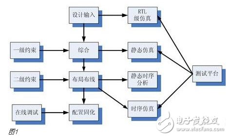
August 05, 2021