Abstract: This paper introduces a design scheme of synchronous high-speed data acquisition based on USB2.0 interface and its software and hardware design methods. It briefly describes the characteristics of Cypress USB2.0 control chip CY7C68013 and synchronous data acquisition chip AD7862. Focus on the design of CPIP and its driver software. With the rapid development of computer technology, the requirements for the speed of external buses are getting higher and higher. Universal Serial Bus (Universal Serial Bus, or USB bus), with its advantages of plug and play, hot swap, and high transmission rate, has become a universal standard for connecting PCs and peripherals. On many portable computers, the RS-232 interface is no longer available. So far, the commonly used USB bus standard has USBl released in 1998. Version 1 and USB2.0 version released in 2000. Version 1.1 supports two transmission rates: 1.5 Mbps and 12 Mbps, which is mainly used in the occasions where low-speed transmission is required; while version 2.0 is for high data rate transmission, it supports 480 Mbps transmission speed and is fully compatible with the downward USBl. 1 agreement. In practical applications, there are usually some burst signals that need to be collected at high speed and data is transferred at high speed, so the USB2.0 standard naturally becomes the first choice. Taking the CY7C68013 chip in the EZ-USB FX2 series of Cypress as the core controller, a set of high-speed synchronous data collectors conforming to the USB2.0 standard was designed and developed. 1 CY7C68013 chip The CY7C68013 in Cypress's EZ-USB FX2 series is one of the few USB controllers on the market that meets the USB2.0 standard. Compared with other similar chips, it provides 4KB FIFO and a very powerful GPIF (General Programmable Interface) module. The latter is equivalent to a programmable state machine. It is precisely because of its existence that CY7C68013 has a stronger interconnection ability than other similar chips. Figure 1 is a schematic diagram of the structure of the CY7C68013 chip. Its main features are as follows: CY7C68013 integrates an enhanced 51 core, its instruction set is compatible with the standard 8051, and has been improved in many aspects. For example: the highest operating frequency can reach 48MHz, one instruction cycle is 4 clock cycles, two UART interfaces, three timer counters, an I2C interface engine, etc. CY7C68013 provides a serial interface engine (SIE), responsible for completing most of the USB2.0 protocol processing work, thereby greatly reducing the workload of USB protocol processing, and provides 4KB FIFO to ensure the need for high-speed data transmission. In order to meet the interconnection needs of various different types of peripherals, a GPIF module is integrated in the chip, allowing users to edit waveforms according to the timing of the peripherals, without requiring complex program descriptions, to ensure GPIF and internal. The coordination work of FIFO realizes the logical connection and high-speed data transmission between the chip and high-speed peripheral equipment. This is quite friendly for developers. The author uses this feature to achieve high-speed synchronous data collection and transmission. 2. The structure of 1 AD7862 AD7862 is a high-speed, low-power, bipolar 12-bit A / D conversion chip introduced by AD Company, which contains two independent fast ADC modules (allowing simultaneous sampling and conversion of two signals) and four analog input signals (VAl, VA2, VBl, VB2), 2.5V internal voltage reference and a 12-bit high-speed parallel interface. The power consumption of the chip is only 60mW during normal operation, and only 50μW when using the power-saving mode, which is undoubtedly an advantage for the USB device with its own power supply. The internal structure of the chip is shown in Figure 2. Each ADC has a two-channel multiplexer. The chip selects VAl, VA2 or VBl, VB2 through address signal A0. When a CONVST signal arrives, it simultaneously converts the two signals selected by address A0. 2. Control timing of 2 AD7862 The control timing of AD7862 is shown as in Fig. 3. In USB2.0 synchronous high-speed data collector, use GPIF to achieve the timing control shown in Figure 3. CONVST is the conversion start signal, and the falling edge triggers the two ADCs to start to replace; the BUSY signal is triggered by the CONVST signal; it becomes and remains in a high electronic state, and it does not return to low level until the two ADCs are converted; Address A0 is used to select two analog signals. The CS signal and RD signal are the chip enable signal and the read enable signal, respectively. When the two are low for the first time, the data converted by the first group of ADCs is read; when the second is high, the data converted by the second group of ADCs is read. It is worth noting that using the AD7862 is that the chip provides a power management function. When the chip reads the second set of data, the CONVST signal continues to remain low and the chip enters sleep mode. At this time, the power consumption of the chip is only 50 μW. This is very important for today's portable devices. Traditional high-speed data acquisition cards generally use PCI bus design, but laptop computers and most portable devices do not have PCI slots. The use of USB2.0 technology not only guarantees a high data transmission rate (the maximum transmission rate can reach 480Mbps), but also has the advantages of being portable and requiring no external power supply. Figure 4 is a schematic diagram of the structure of the system. Its working principle is: under the control of the GPIF module, the AD7862 samples the target at equal intervals, and then transmits the sampling result to the internal FIFO buffer of CY7C68013 through GPIF; when a certain amount of data is collected, CY7C68013 automatically packs the data (No need for 8051 intervention), transfer to PC through USB bus for data processing. Because of the GPIF hardware support, the 8051 core in CY7C68013 only assists the control in a very short time, and most of the work is done by the GPIF hardware. In this way, the 8051 can also interconnect with other peripherals. Two RS-232 interfaces are added to the high-speed data collector, which is used to transfer GPS data and high-precision intelligent sounder data to the main control computer, which greatly facilitates the recently launched notebook computer and traditional peripherals. Connection. Most of the newly launched notebook computers do not have RS-232 interface, and most of the field observation instruments can only exchange data through the RS-232 interface. For CY7C68013, its configuration and firmware are soft, stored in external E2PROM, and automatically loaded from the I2C bus to the on-chip RAM at power-on. It is very convenient to modify and facilitate firmware upgrade. Because CY7C68013 provides abundant I / O ports, it is also very convenient to expand functions, such as adding a GPIB data port. 4 Software design The software design of the USB device includes three aspects: firmware design, hardware driver design and advanced application design. 4.1 Firmware (firmware) design Cypress provides a development framework for CY7C68013, which can be developed under KEIL C51 environment. Due to the introduction of the development framework, the user's research and development cycle has been greatly shortened. The framework consists of the following parts: (1) FW. C contains the MAIN function of the program framework to manage the operation of the entire 51 core, because Cypress has carefully divided the functions of this part, and generally does not need to be changed. · TD_Init function, responsible for initial setting of USB endpoint. In this design, the endpoint 6 is set to 1024 bytes, the buffer depth is level 4, and the mode is set to automatic input. · TD_Poll function, responsible for the processing of cyclic tasks in the system. It mainly inquires about the status of each endpoint and handles the interaction of various OUT or IN endpoints. It is worth noting that this process is only auxiliary and most of the work is done automatically by the hardware. The DR_VendorCmnd function is mainly responsible for the decoding of user-defined commands. User requests are transmitted to the kernel through the endpoint O. Due to the support of SIE hardware on CY7C68013, users only need to query the fixed address unit to obtain the current command code. · GPIFINIT. C, there is only one Gpiflnit function; it is the initialization function of the GPIF module, which is generally called in the TD_Init function. This function is generated by a GPIF Designer development tool provided by Cypress based on the user-designed waveform. The user does not need to design the waveform look-up table, which reduces the designer's work intensity. · DSCR. A51 is a description table file, which is responsible for the description of the USB device. CY7C68013 automatically uses the VID and PID to replace the default VID and PID after power on. · Two included files EZUSB. LIB and USBJMPTB. OBJ, the former is the binary file of the EZUSB function library, and the latter is the USB interrupt vector table. For firmware debugging, use the EZ-USB control panel provided by Cypress. For specific operation readers can refer to its own help. 4.2 Design of driver The driver is responsible for access to the underlying hardware. In the driver development of this design, the development tool used is WinDriverv6.03 of Jungo Company, which supports multiple operating systems. The advantage of using WinDriver development is that users do not need to understand the specific working mechanism of the operating system, and they do not need to understand the development tools of DDK (Developing or Debugging in Kernel) of each system. Users only need to use the development platform provided by WinDriver to complete Driver design work, the remaining low-level details are handled uniformly by the WinDriver kernel, thereby reducing the requirements for developers' programming ability, and also greatly shortening the development cycle. The following is a brief description of the steps for using WinDriver to develop a driver program (taking development under the Windows operating system as an example): (1) Start the DriverWizard tool of WinDriver; (2) Use DriverWizard to check whether the hardware is normal; (3) Select the development environment used in DriverWizard, here use VB6.0 development environment, and generate driver code; (4) Modify the generated code to make it meet the needs of the system; (5) In the user mode of the WinDriver environment, debug the driver; (6) If the program needs kernel access to improve the efficiency of the driver, enter the kernel development. The high-level application is built on the driver. In this design, the development environment of VB6.0 is selected to develop the application. It uses the driver as a bridge to control the USB device and process the data returned by the USB device, such as waveform display and spectrum analysis. Developers can make a control or data packet of a USB controller according to their actual needs, and connect or embed it into the application when writing the application. With the rapid popularity of notebook computers, high-performance portable collectors will attract much attention, especially now that the RS-232 interface has been abandoned by most notebook computers, the demand for USB data collectors has become more urgent, and Has shown good market prospects. The high-speed synchronous data collector based on USB2.0 described in this article is not only limited to data acquisition in terms of its function, but also a powerful mixed-signal processor. The use of underwater robot sonar and Zhejiang deep-water cage monitoring equipment shows that the data throughput is large and the performance is stable, which meets the design requirements. As long as it is equipped with a suitable sensor and corresponding signal conditioning circuit, the high-performance collector described in this article can be used to collect and analyze various analog quantities. If it can be matched with appropriate firmware design, it can constitute a multi-function control system. Signal Scaling: It adjusts the input signal resolution to match the resolution of the LED screen. For example, if a 4K signal is fed to a screen with a different native resolution, the processor will scale it appropriately. Color Calibration and Correction: Video processors often include tools for color correction to ensure that the colors displayed on the LED screen match the intended output, accounting for any discrepancies in the LED panels’ color reproduction. Image Enhancement: They improve the visual quality by adjusting brightness, contrast, sharpness, and other image settings to make the picture look more vibrant and clear. Edge Blending: For large or curved displays made up of multiple LED panels, processors can blend the edges of each panel so that the transition between panels is seamless, eliminating visible lines or "joints." Frame Synchronization: It ensures that the input signal is synchronized with the LED display’s refresh rate to avoid issues like screen tearing or stuttering. Video Wall Management: In the case of multi-screen video walls, a video processor manages the distribution of the content across all screens, ensuring proper alignment, scaling, and synchronization. Input and Output Flexibility: Modern video processors come with multiple inputs (HDMI, DisplayPort, SDI, DVI, etc.) and outputs for compatibility with various sources and LED screen types. Video Signal Conversion: Converting between different types of video signals (e.g., from analog to digital) and ensuring the display can handle different formats, frame rates, and resolutions. Video Format and Aspect Ratio Handling: The processor manages and adjusts various video formats and aspect ratios to ensure the content fits properly on the LED display without distortion or cropping. Basic Video Processors: Used for small-scale applications like single LED displays or basic content delivery, often providing simple scaling and color correction. Advanced Video Processors: These are designed for large-scale, high-performance LED installations (such as digital signage, control rooms, or live events). They offer features like 4K/8K resolution support, advanced color calibration, and multi-channel input/output. LED Video Wall Processors: Tailored for large LED video walls, these processors manage complex content, control panel configurations, and allow for the flexible distribution of content across multiple screens. Novastar: Known for its powerful processors that are commonly used in large-scale LED screens, providing tools for scaling, color calibration, and signal management. Linsn: Specializes in LED display solutions, including video processors for high-end applications like video walls and stadium screens. Datapath: Offers advanced video processing solutions for professional-grade LED walls, including high-end video and graphics cards. Colorlight: Known for both hardware and software solutions that include LED display control systems, processors, and scalers. Barco: Provides high-performance processors often used in professional AV applications, with a focus on video wall management and color accuracy. Kramer: Offers a wide range of video processors for different types of installations, from small to large-scale LED screens. When choosing a video processor for an LED screen, consider the following factors: Let me know if you'd like more specific product recommendations or details on how to integrate these processors into your system! Controller,video processor,led display controller Guangzhou Chengwen Photoelectric Technology co.,ltd , https://www.cwleddisplay.com
figure 1
2 Synchronous high-speed data acquisition chip AD7862 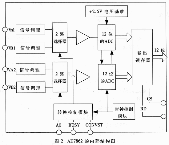
3 Hardware design of synchronous high-speed data collector
image 3
(2) The user must put PERIPH. C is instantiated, it is responsible for interconnection of peripheral devices in the system. The design of the firmware is mainly aimed at this file. The user must instantiate this file according to the needs of his system to realize his own functions. There are several functions in this file that are more critical. Here are some special instructions: 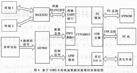
4.3 Design of advanced applications
Types of LED Video Processors:
Examples of Popular LED Screen Video Processor Brands:
Common Applications:
A LED screen video processor is an essential component used to control, manage, and optimize the video signal for LED Display panels, ensuring high-quality image rendering, accurate color reproduction, and smooth video playback. It acts as an intermediary between the video source (e.g., computer, media player, camera, etc.) and the LED screen, handling tasks like signal conversion, scaling, synchronization, and color correction.
Key Functions of a Video Processor for LED Screens:
May 29, 2025