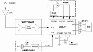
Pick   To:       This article discusses the down-conversion technology in the handheld software radio platform, and compares the advantages and disadvantages of direct down-conversion and superheterodyne structure. The direct down conversion module with AD8347 as the core is introduced in detail , and its example application is given. introduction Software radio is a new type of radio processing technology developed with the rapid development of computer technology and high-speed digital signal processing technology. The basic idea is to bring the wideband A / D and D / A converters as close to the antenna as possible, and to implement the various functions of the radio as far as possible on an open, modular platform by software, with strong flexibility and Upgradability. The emergence of software radio has brought radio technology from an era dominated by hardware to an era dominated by software. It is the third generation of wireless communication technology after analog communication technology and digital communication technology. An ideal software radio platform samples directly on the radio frequency signal, but due to the limitations of the technical level of broadband antennas, high-speed A / D and DSP , the conditions for achieving such an ideal platform are not yet available, and can only be done at intermediate frequency or baseband Sampling. Therefore, the current research on software radio is more about studying how to achieve the versatility and flexibility required by software radio to the greatest extent under the existing technical conditions, and embodying the design ideas of software and generalization to specific In practice. FIG. 1 shows a spread spectrum communication handheld platform based on software radio thinking in baseband signal sampling processing. Picture 1  Block diagram of the software radio handheld platform of the direct sequence spread spectrum receiver  Picture 2  Structural block diagram of the RF direct down conversion module Picture 3  Block diagram of DSP module of software radio platform As can be seen from Figure 1 , the platform is mainly divided into two parts: the analog front end of the RF reception and the DSP processing module. The spread spectrum signal bandwidth of the system is above 5MHz . For the RF module of the handheld platform, under the condition of limited power consumption and volume, how to down-convert the broadband signal from the RF to the baseband for processing is stable and accurate. difficulty. In response to this difficulty, the author uses direct down-conversion technology to solve this problem. Method for realizing down conversion The basic principle of down-conversion is to mix and filter the RF modulated signal and move it to a lower frequency band or baseband for processing. There are two main implementation methods: (1) superheterodyne structure; (2) direct down conversion frequency conversion. The superheterodyne structure has a two-level or multi-level down-conversion process, and finally the signal is demodulated at low intermediate frequency or baseband; while the direct down conversion technology eliminates the intermediate frequency conversion link and directly performs the received RF modulation signal once Frequency down-conversion demodulation to obtain the baseband signal. Comparing the two, direct down conversion is an ideal RF signal processing solution, which has been expected by wireless communication engineers. However, due to the limitations of the manufacturing process and the size of the components, this method has not been specifically promoted for a long time, but the superheterodyne structure scheme is generally selected. However, for handheld devices that emphasize size and power consumption, the superheterodyne structure has significant problems compared with direct down conversion: Compared with the superheterodyne structure, direct down conversion processing also has some weaknesses: The weaknesses in these circuits can be effectively solved through careful design and debugging, at a relatively low cost. In summary, using direct down-conversion technology to directly convert the RF signal to baseband for processing, it can save the multi-level intermediate frequency circuit and can reduce the number of peripheral components, cost, power consumption, printed circuit board area and design complexity , Suitable for applications on handheld devices.            Direct down conversion module of software radio platform The platform's direct down-conversion module is built with AD8347 as the core, and completes the signal movement from RF to baseband. AD8347 is a single-chip direct-conversion wideband quadrature demodulator IC from Analog Devices , capable of receiving RF input in the range of 800MHz to 2.7GHz and directly downconverting the input signal to baseband in-phase / quadrature components The AC component is sent to a high-speed ADC for digitization. The AD8347 integrates on-chip RF and baseband controllable gain amplifiers to provide a variable gain range of 70dB , making it easy to implement complex wide dynamic range reception designs. At the same time, it has 50MHz output demodulation bandwidth, which can meet the requirements of GSM , CDMA and the latest 3G communication bandwidth. Its signal output has excellent phase and amplitude balance, quadrature phase accuracy can reach 1 °, I / Q amplitude imbalance is controlled within 0.3dB ( ie 3.5%) , so it can be used for wireless local loop and microwave radio connection Provide an economical direct frequency conversion solution. In addition, the AD8347 also integrates a buffered local oscillator driver that only requires a drive level of -10dBm , a baseband level detector, a DC offset zeroing circuit, and a dual-channel differential output amplifier with adjustable DC common-mode level, which can directly Drive a variety of dual-channel ADCs , such as AD9201 , AD9218, etc. Figure 2 shows the block diagram of the RF direct down-conversion module with AD8347 as the core. It is mainly divided into 4 parts: AD8347 module, low-noise amplifier, local oscillator frequency synthesis circuit and AGC circuit. Low noise amplifier A low-noise amplifier with a gain of 30dB and a noise figure of 1.5dB is selected, which has a large dynamic range, and P-1dB is -3dBm . In mechanical structure and circuit design, it is necessary to pay attention to deal with it and other circuits Mutual shielding, especially the isolation from the local oscillator generating circuit. The better the isolation is, the more likely it is that the RF signal amplifier will be blocked due to local oscillator leakage. Local oscillator frequency synthesis circuit The local oscillator signal is obtained by TCXO phase-locked frequency multiplication, and the LMX2347 frequency synthesis chip of NS is used . This oscillation circuit is to be noted in the design size of the output level, the recommended control -8dBm about ADI recommended, while paying attention to the mask processing and design compatibility. AGC circuit This system adopts the spread spectrum system, which requires high receiving sensitivity, and the baseband signal bandwidth is about 5MHz . The thermal noise input by the antenna is ideally: -174 (dBm / Hz) * 5 (MHz) =-107 dBm Under normal working conditions, the signal strength is much lower than the thermal noise level, and the signal-to-noise ratio reaches -20dB . Select non-correlated AGC to control the final output signal amplitude to 2VP-P . During the design, pay attention to control the starting point of the AGC so that it covers the possible signal input strength range during specific work. DSP module of software radio platform DSP Software Radio module as a data acquisition and processing core, including the ADC, FIFO and DSP, FIG. 3 is the thinning of the DSP core of the module of FIG. The bandwidth of the spread spectrum communication in the system is 5MHz . AD8347 moves the broadband signal modulated on the radio frequency 2.2GHz to the near-zero intermediate frequency band, which is divided into two orthogonal signal outputs of I and Q channels. Then the I and Q signals are sampled by A / D at a sampling rate of 20M / s . Finally, the data sampled by the A / D is passed to the DSP through the FIFO for demodulation and despreading. The AD9201 in Figure 3 is a dual-channel, low-voltage, high-speed A / D from Analog Devices . The sampling rate of each channel can reach 20M samples per second . Its accuracy is stable and reliable, and within the full sampling bandwidth, the accuracy always maintains a 10 -bit accuracy. Its working voltage setting is quite flexible, allowing to change in the range of 2.7V ~ 5.5V , especially suitable for high-speed operation of portable devices at low voltage. The analog signal can be input differentially or single-ended to ground. The peak -to- peak value of the signal is usually set to 1Vp-p or 2Vp-p . VREF is the reference power supply output of the AD9201 , which is stable at 1V , providing an accurate voltage offset reference for the AD8347 . Processor core member is ADI's ADSP BF533, the DSP is ADI and Intel jointly launched the company in early 2003 of a fixed-point DSP, belonging to the new Blackfin family. BF533 has RISC instruction structure, efficient operation and excellent performance. It runs on a 600MHz frequency, having two 40 bit MAC and the two 32 bit ALU, 10 addressable unit address. The DSP integrates 148 k Byte of full-speed RAM , and has a wealth of external interfaces, such as SPI , synchronous and asynchronous serial ports, watchdogs, and various timers. It is worth mentioning that the BF533 power control is good, the power consumption is only 280mW at the main frequency of 600MHz , and can dynamically control the voltage input, adjust the operating frequency, reduce chip power consumption, very suitable for mobile product design. FIFO is used as an external high-speed data cache to ensure the normal operation of the system timing. The depth is 32K words, and the response speed is above 100M Hz / s . The write clock WCLK is 40MHz , and the dual-channel high-speed data collected by the AD9201 is read in time . The read clock RCLK is controlled by BF533 , performs DMA transfer, and works stably at more than 50M words / second. FIFO provides half full flag signal / HF to DSP to ensure that the data is not filled and read empty.       System index analysis The measured index of the RF direct down conversion module with AD8347 as the core is shown in Table 1 . From the test results in the table, it basically agrees with the technical parameters given by ADI . From the point of view of the DSP module, the highest signal-to-noise ratio of the zero-IF signal output from the AD8347 is about 30dB , and the lowest signal-to-noise ratio is about -20dB . In a strong signal-to-noise ratio environment, for the baseband spread spectrum signal, the DSP module despreading effect is ideal, without error codes. In the environment with the lowest signal-to-noise ratio , the bit error rate of the DSP module after despreading is about 10-5 , which achieves the intended purpose of system design. Conclusion Engineering practice has proved that the software radio processing platform of the entire system has a reasonable structure and stable performance. Because the tiny packaged integrated circuits are used as much as possible, the size of the receiver is only slightly larger than that of the business card, and the power consumption is less than 1 watt, which satisfies the need of carrying on the palm. The software has a modular design, is easy to upgrade, has strong portability and compatibility, and can be applied to many aspects such as 3G test equipment and satellite communications. The platform has been successfully applied in a communication system, and the system operation results meet the technical requirements. 60 Port Usb Charger,Multi-port USB 600W charger,60 Port Usb Smart Charger,High Power Mobile Phone Charger shenzhen ns-idae technology co.,ltd , https://www.best-charger.com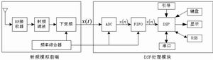


60 Port USB Charging
This 60 -port USB charger is charged at the fastest speed to as many as 60 devices. The table charger has 60 ports. The maximum output of a single USB port is 2.4A, and the output power is as high as 300W. Super intelligence: Each port can charging a current of up to 2.4A, and adaptive smart chip detector can provide the best charging current for connected devices. Multiple protection: The USB charger has rush protection, over -current and overvoltage protection functions, which can safely protect your smart devices. Suitable for multiple devices: charging stations are compatible with 99 % of smart devices, such as iPad iPhone, tablet, Bluetooth headset, fan, DVS, for PSP. It is suitable for various occasions, such as hotels, school dormitories, gym and other places.
May 28, 2025